Transparent Electrode for Semiconductor Light-Emitting Device

a technology of light-emitting devices and transparent electrodes, which is applied in the direction of semiconductor devices, basic electric elements, electrical appliances, etc., can solve the problems of high specific resistance of type gan compound semiconductors, increase in contact resistance, and rise of forward voltage (vsub>f/sub>), and achieve excellent ohmic contact, reduce resistance magnitude, and fast adhesion

Active Publication Date: 2008-02-21
TOYODA GOSEI CO LTD
View PDF9 Cites 17 Cited by
  • Summary
  • Abstract
  • Description
  • Claims
  • Application Information

AI Technical Summary

Benefits of technology

[0019] The transparent electrode of this invention has a p-type semiconductor layer, a contact metal layer formed on the p-type semiconductor layer, a current diffusion layer formed on the contact metal layer and a bonding pad formed on the current diffusion layer. The contact metal layer is formed of a material possessing transparent property and acquiring excellent ohmic contact. The current diffusion layer is formed of a material possessing a lower magnitude of resistivity on the plane of the transparent electrode than the contact metal layer. The bonding pad is formed of a material giving rise to fast adhesion to the current diffusion layer. Therefore, the configuration obtained will bring an effect of enlarging the light-emitting plane in the semiconductor layer, decreasing the operation voltage in the forward direction and providing the bonding pad with excellent adhesive strength.

Problems solved by technology

Further, the p-type GaN compound semiconductor has high specific resistance as compared with the n-type GaN compound semiconductor and is not hardly enabled by simply stacking metal on the first surface to add to the lateral expanse of electric current in the p-layer and, when fabricated in an LED configuration having a p-n junction, is enabled to emit light only directly below the positive electrode.
When a bonding pad is allowed to contact a semiconductor layer, the contact entails the problem that the part of this contact inevitably gives rise to an increase in the contact resistance and consequently suffers the forward voltage (VF) to rise.

Method used


Image

  • Transparent Electrode for Semiconductor Light-Emitting Device
  • Transparent Electrode for Semiconductor Light-Emitting Device
  • Transparent Electrode for Semiconductor Light-Emitting Device

Examples


example 1

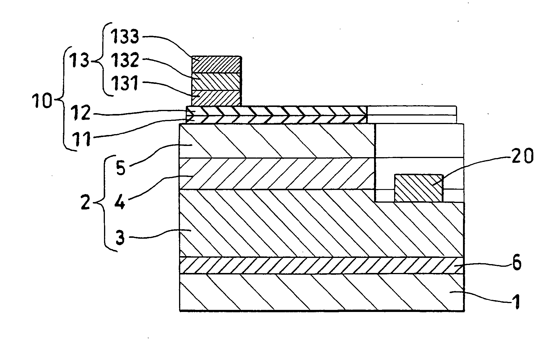
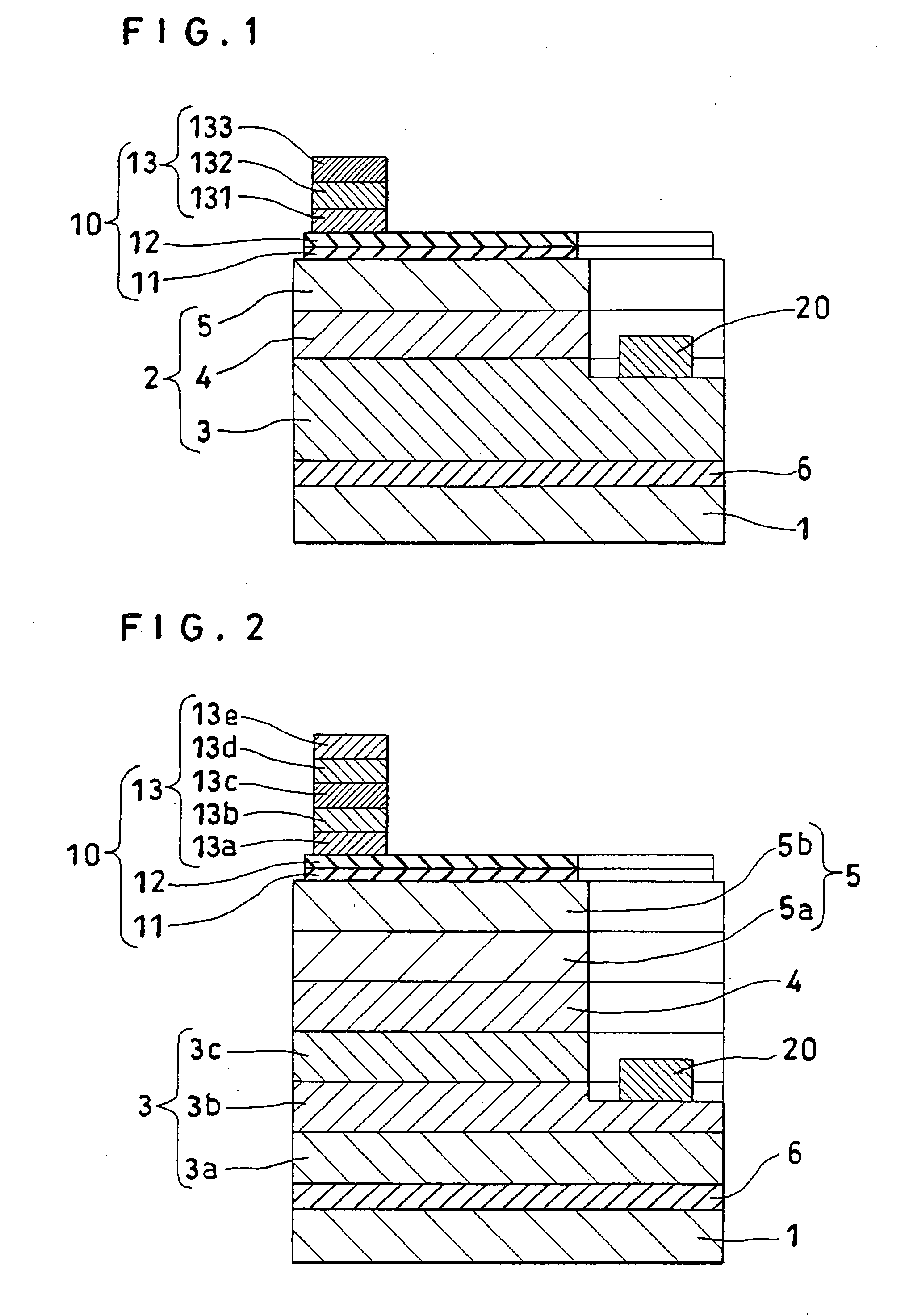
[0057]FIG. 2 is a schematic view illustrating the cross section of a gallium nitride-based compound semiconductor light-emitting device fabricated in this example and FIG. 3 is a schematic view illustrating the plan view thereof. On a substrate 1 made of sapphire, an under layer 3a made of undoped GaN and measuring 8 μm in thickness, an Si-doped n-type GaN contact layer 3b measuring 2 μm in thickness, an n-type In0.1Ga0.9N cladding layer 3c measuring 250 nm in thickness, a Si-doped GaN barrier layer measuring 16 nm and an In0.2Ga0.8N well layer measuring 1.5 nm in thickness were stacked through a buffer layer 6 made of AlN up to five repetitions. Finally, a positive electrode 10 of this invention formed of a bonding pad layer 13 of a five-layer structure consisting of a Pt contact metal layer 11 measuring 1.5 nm in thickness, an Au current diffusion layer 12 measuring 5 nm in thickness, an Au layer 13a measuring 50 nm in thickness, a Ti layer 13b measuring 20 nm in thickness, an Al ...

example 2

[0071] In Example 2, an electrode was formed in the following structure with a substrate having the same stacked structure as in Example 1.

[0072] Specifically, a positive electrode 10 of this invention was formed of a bonding pad 13 in a five-layer structure consisting of a Pt contact metal layer 11 measuring 1.5 nm in thickness, an ITO current diffusion layer 12 measuring 100 nm in thickness and a Cr layer 13a measuring 50 nm in thickness, a Ti layer 13b measuring 20 nm in thickness, an Al layer 13c measuring 10 nm in thickness, a Ti layer 13d measuring 100 nm in thickness and an Au layer 13e measuring 200 nm in thickness. In the five layers which formed the bonding pad, the Cr layer 13a measuring 50 nm in thickness constituted a first layer, the Ti layer 13b measuring 20 nm in thickness a second layer, the Al layer 13c measuring 10 nm in thickness a barrier layer, the Ti layer 13d measuring 100 nm in thickness a layer for preventing Al and Au from being alloyed, and the Au layer ...


PUM


Abstract

A transparent electrode for a gallium nitride-based compound semiconductor light-emitting device includes a p-type semiconductor layer (5), a contact metal layer (1) formed by ohmic contact on the p-type semiconductor layer, an current diffusion layer (12) formed on the contact metal layer and having a lower magnitude of resistivity on the plane of the transparent electrode than the contact metal, and a bonding pad (13) formed on the current diffusion layer. The transparent electrode is at an advantage in widening the surface of light emission in the p-type semiconductor layer, decreasing the operation voltage in the forward direction, and enabling the bonding pad to provide excellent adhesive strength.

Description

CROSS REFERENCE TO RELATED APPLICATIONS [0001] This application is an application filed under 35 U.S.C. §111(a) claiming the benefit pursuant to 35 U.S.C. §119(e)(1) of the filing dates of Provisional Application No. 60 / 602,648 filed Aug. 19, 2004 and Japanese Application No. 2004-228968 filed Aug. 5, 2004 pursuant to 35 U.S.C §111 (b).TECHNICAL FIELD [0002] This invention relates to a transparent electrode and more particularly to a transparent electrode possessing excellent transparent property and ohmic property suitable for a gallium nitride-based compound semiconductor light-emitting device. BACKGROUND ART [0003] In recent years, the GaN-based compound semiconductor materials have been attracting attention as semiconductor materials for use in the short wavelength light-emitting devices. The GaN-based compound semiconductors are formed on sapphire single crystals and various oxides and Group III-V compounds as substrates by the metal organic chemical vapor deposition method (MO...

Claims


Application Information

Patent Timeline
Patent Type & Authority Applications(United States)
IPC IPC(8): H01L33/00H01L21/28H01L33/06H01L33/14H01L33/32H01L33/42
CPCH01L33/42H01L33/32
Inventor EITOH, NOBUOMURAKI, NORITAKAMIKI, HISAYUKIWATANABE, MUNETAKA
Owner TOYODA GOSEI CO LTD
Why Eureka
Try Eureka