Intersubband quantum box stack lasers

a quantum box and stack laser technology, applied in the field of semiconductor lasers, can solve the problems of low radiative efficiency, low confinement, low efficiency of wall plugs, etc., and achieve the effects of improving confinement, long-range coherent coupling, and preferential enhancement of modal gain

Active Publication Date: 2008-02-21
WISCONSIN ALUMNI RES FOUND
View PDF48 Cites 14 Cited by
  • Summary
  • Abstract
  • Description
  • Claims
  • Application Information

AI Technical Summary

Benefits of technology

[0017]The laterally periodic waveguide may be created due to periodic variations in the thicknesses of one optical confinement layer and one cladding layer adjacent to the optical confinement layer which in turn lead to alternating low-effective-index and high-effective-index regions in the waveguide, whereby the low-effective-index regions define laser device elements and the high-effective-index regions define interelement regions, whereby modal gain is preferentially enhanced in the laser device elements, thereby insuring that only the APC-structure modes peaked in those regions can lase and allowing for long range coherent coupling via traveling waves.
[0018]In one embodiment based on a GaAs material system, the waveguide may include optical confinement layers of n-GaAs adjacent to the laser core and outer cladding layers of n+-GaAs. The waveguide may optionally also include additional cladding layers, such as an AlGaAs and / or InGaAs layers to improve confinement.

Problems solved by technology

However, the basic limitation, low radiative efficiency, was not improved, since phonons still dominate the level 3 to level 2 transition.
However, that was achieved with very low wallplug efficiency, ηp, values (<1%) and highly temperature-sensitive characteristics.
This poor performance is directly related to the fact that the rise in the active-region temperature with respect to the heatsink temperature is very high (e.g., 70-80° C.
However, due to relatively low gain, such devices will provide low powers (˜30 mW) from conventional single-element devices.
Since QCLs may utilize a buried heterostructure design in order to assist with lateral heat removal, it is impractical to incorporated such lasers into APC structures for scaling the power, as it is done for other types of lasers.

Method used


Image

  • Intersubband quantum box stack lasers
  • Intersubband quantum box stack lasers
  • Intersubband quantum box stack lasers

Examples


Embodiment Construction

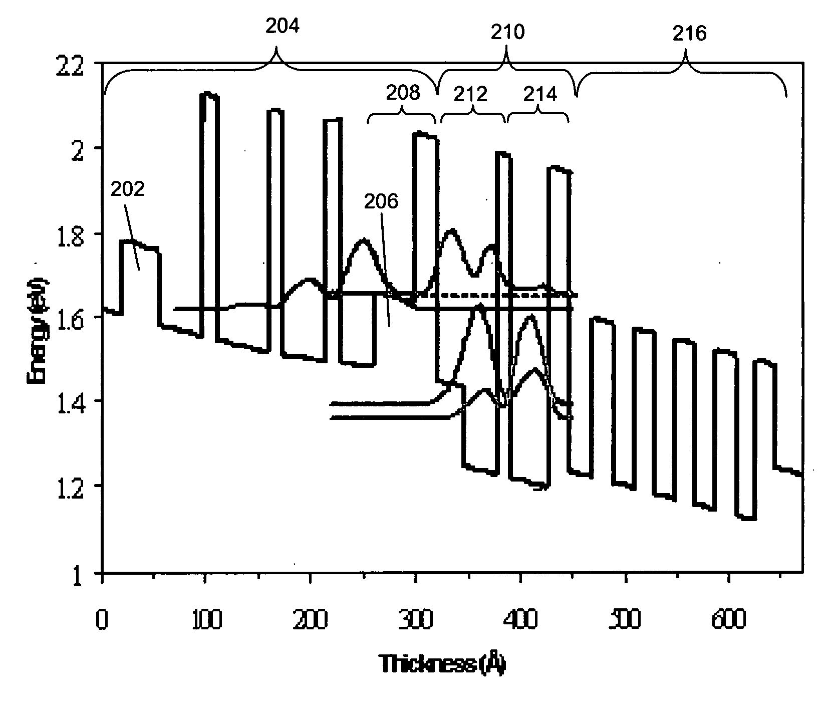
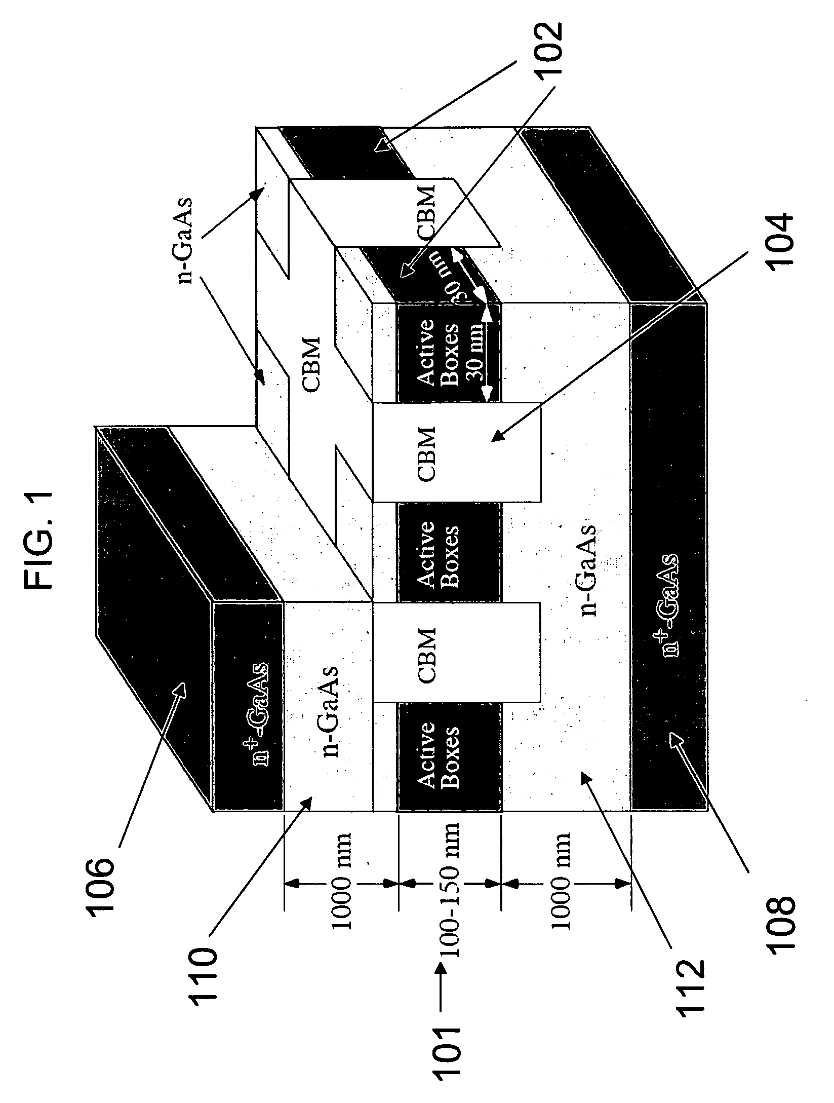
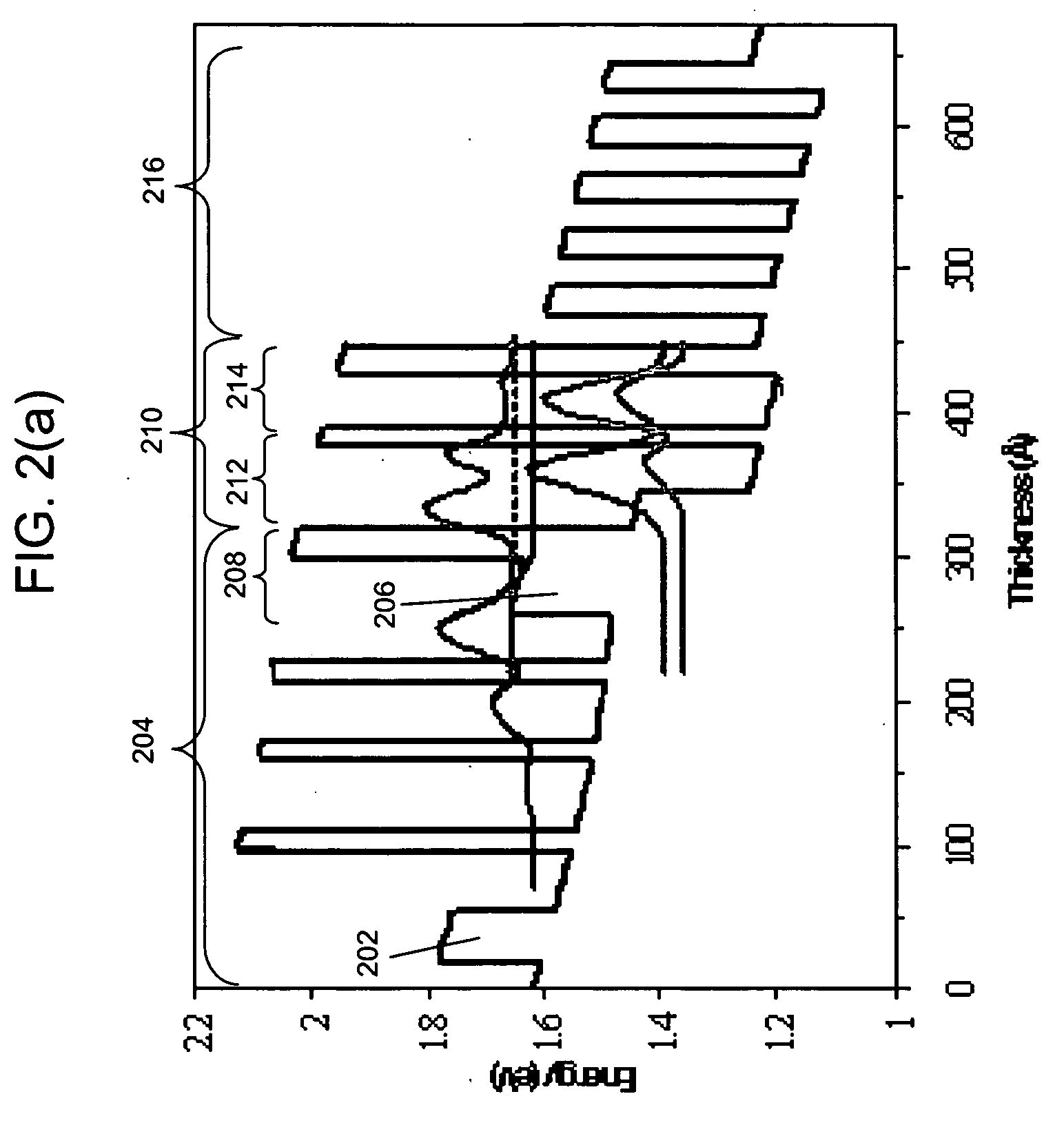
[0032]The present invention provides semiconductor lasers having an APC structure that allows scaling of the coherent power by using a waveguide having a periodic structure that selects operation in a single spatial mode from large-aperture devices. The lasers include an active medium that includes an array of quantum box ministacks, each ministack containing 2 to 5 vertically stacked, coupled quantum boxes.

[0033]The present lasers are capable of providing an output power of at least about 0.5 Watts (W). This includes embodiments that provide an output power of at least about 1 W, further includes embodiments that provide an output power of at least about 5 W and still further includes embodiments that provide an output power of at least about 10 W. The lasers are also capable of providing a wallplug efficiency of at least about 30%, and may operate at low temperatures (e.g., room temperature (˜30° C.) operation). In some embodiments the lasers have a wallplug efficiency of at least...


PUM


Abstract

The present invention provides semiconductor lasers having an Active-Photonic-Crystal (APC) structure that allows scaling of the coherent power by using a waveguide having a periodic structure that selects operation in a single spatial mode from large-aperture devices. The lasers include an active medium that includes an array of quantum box ministacks, each ministack containing 2 to 5 vertically stacked, coupled quantum boxes.

Description

STATEMENT OF GOVERNMENT RIGHTS[0001]Research funding was provided for this invention by the National Science Foundation under grant No. NSF: 0200321. The United States government has certain rights in this invention.FIELD OF THE INVENTION[0002]This invention relates to semiconductor lasers incorporating arrays of stacked quantum boxes in an active photonic crystal structure.BACKGROUND OF THE INVENTION[0003]Semiconductor lasers are formed of multiple layers of semiconductor materials. The conventional semiconductor diode laser typically includes an n-type layer, a p-type layer and an undoped layered active structure between them such that when the diode is forward biased electrons and holes recombine within the active structure with the resulting emission of light. The layers adjacent to the active structure typically have a lower index of refraction than the active structure and form cladding layers that confine the emitted light to the active structure and sometimes to adjacent lay...

Claims


Application Information

Patent Timeline
Patent Type & Authority Applications(United States)
IPC IPC(8): H01S5/00
CPCB82Y20/00H01S5/105H01S5/3412H01S5/3402H01S5/2004H01S5/11
Inventor BOTEZ, DAN
Owner WISCONSIN ALUMNI RES FOUND
Why Eureka
Try Eureka