Solid-state imaging device

a solid-state imaging and imaging device technology, applied in the direction of radio frequency controlled devices, instruments, television systems, etc., can solve the problems of high brightness the deviation of the black level between the right and left sides of the subject, and the inability to secure a sufficient manufacture tolerance, so as to reduce the variation of the electric current, reduce the influence of other column amplifiers, and ensure the effect of operation

Inactive Publication Date: 2008-02-28
COLLABO INNOVATIONS INC
View PDF4 Cites 6 Cited by
  • Summary
  • Abstract
  • Description
  • Claims
  • Application Information

AI Technical Summary

Benefits of technology

[0013]According to this configuration, using an electric current generated by the current generating circuit, the solid-state imaging device according to the present invention can reduce a variation in an electric current that flows between a column amplifier power supply and a ground without exerting an influence upon characteristics of the column amplifier. Thus, a solid-state imaging device can be realized that, even when capturing an image of a subject with high brightness, prevents the occurrence of a deviation in black level at a periphery of the subject, and has high manufacture and operation tolerances.
[0014]In the above-described solid-state imaging device according to the present invention, it is preferable that, with respect to a current value that is a sum of values of the operation current and the correction current, a variation in the current value that occurs in accordance with a level of an input signal inputted to each of the plurality of column amplifiers is smaller than a variation in the operation current. According to this configuration, when an operation current of a column amplifier changes due to an input signal of the column amplifier, such as when an image of a subject with high brightness is captured, the influence upon other column amplifiers can be reduced reliably.
[0015]Furthermore, in the solid-state imaging device according to the present invention, it is preferable that a bias potential generating circuit that applies a bias potential to the current generating circuit has a circuit configuration similar to a circuit configuration of each of the plurality of column amplifiers. According to this configuration, an electric current generated in a current generating circuit in accordance with a variation in operation current of a column amplifier can be controlled easily.
[0016]Moreover, it is preferable that: in accordance with a potential at one or a plurality of nodes in each of the plurality of column amplifiers, the current generating circuit switches between two or more levels of the correction current; levels of the correction current are switched relative to an output of the bias potential generating circuit; and the current generating circuit is configured so that a constant electric current is passed through the current generating circuit. According to these configurations, a current generating circuit can be adjusted easily and reliably.
[0017]In addition, it is preferable that: a function of switching between ON / OFF states of the current generating circuit itself is provided; the ON / OFF states of the current generating circuit itself are switched based on a level of an input signal or an output signal of each of the plurality of column amplifiers; and the device further includes an analog signal processing portion that includes a gain function and a control portion that controls the device as a whole, and the ON / OFF states of the current generating circuit itself are switched in accordance with gain setting by the analog signal processing portion. According to these configurations, power consumption in a current generating circuit can be reduced.

Problems solved by technology

Then, in each of these column amplifiers in the peripheral portion, a difference in applied voltage may occur between when a reset signal V1 is inputted and when an optical signal V2 is inputted, resulting in the occurrence of a deviation in amplifier output to cause a deviation in black level between the right and left sides of the subject with high brightness, which has been disadvantageous.
However, other problems may occur such as an operation range of the column amplifier being narrowed due to a variation in threshold value of the clip transistor, and characteristics changing when an output of the column amplifier approaches a clip level, thus making it difficult to secure a sufficient manufacture tolerance.
Moreover, it also has been disadvantageous in that photoelectric conversion characteristics also may change as a result of a variation in threshold value due to a variation in ambient temperature.

Method used


Image

  • Solid-state imaging device
  • Solid-state imaging device
  • Solid-state imaging device

Examples


first embodiment

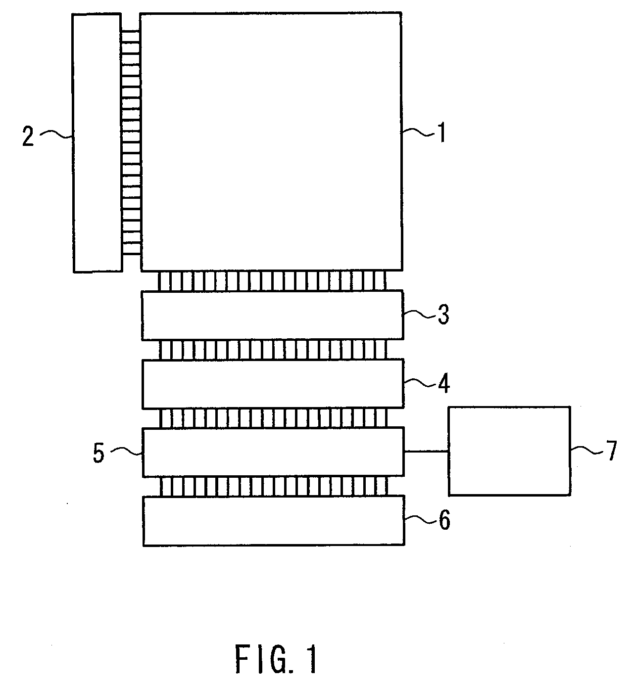
[0036]FIG. 1 is a block diagram of a solid-state imaging device according to a first embodiment of the present invention.

[0037]In a pixel array 1 in which imaging pixels are arranged in a matrix form, a resetting operation, a charge accumulation operation, and a readout operation are performed on a row-by-row basis by a vertical shift register 2. Herein, each of the signals read out on the row-by-row basis is amplified by a column amplifier that is disposed in a column amplifier-arranged portion 3 in a one-to-one correspondence with a signal line in each column, and a value obtained by canceling offset variations of the amplifier is kept in a noise canceling circuit 4. Every set of pixel signals obtained from one row, which has been kept in the noise canceling circuit 4, is selected by a horizontal shift register 6 and is outputted sequentially via a multiplexer 5 and an output amplifier 7.

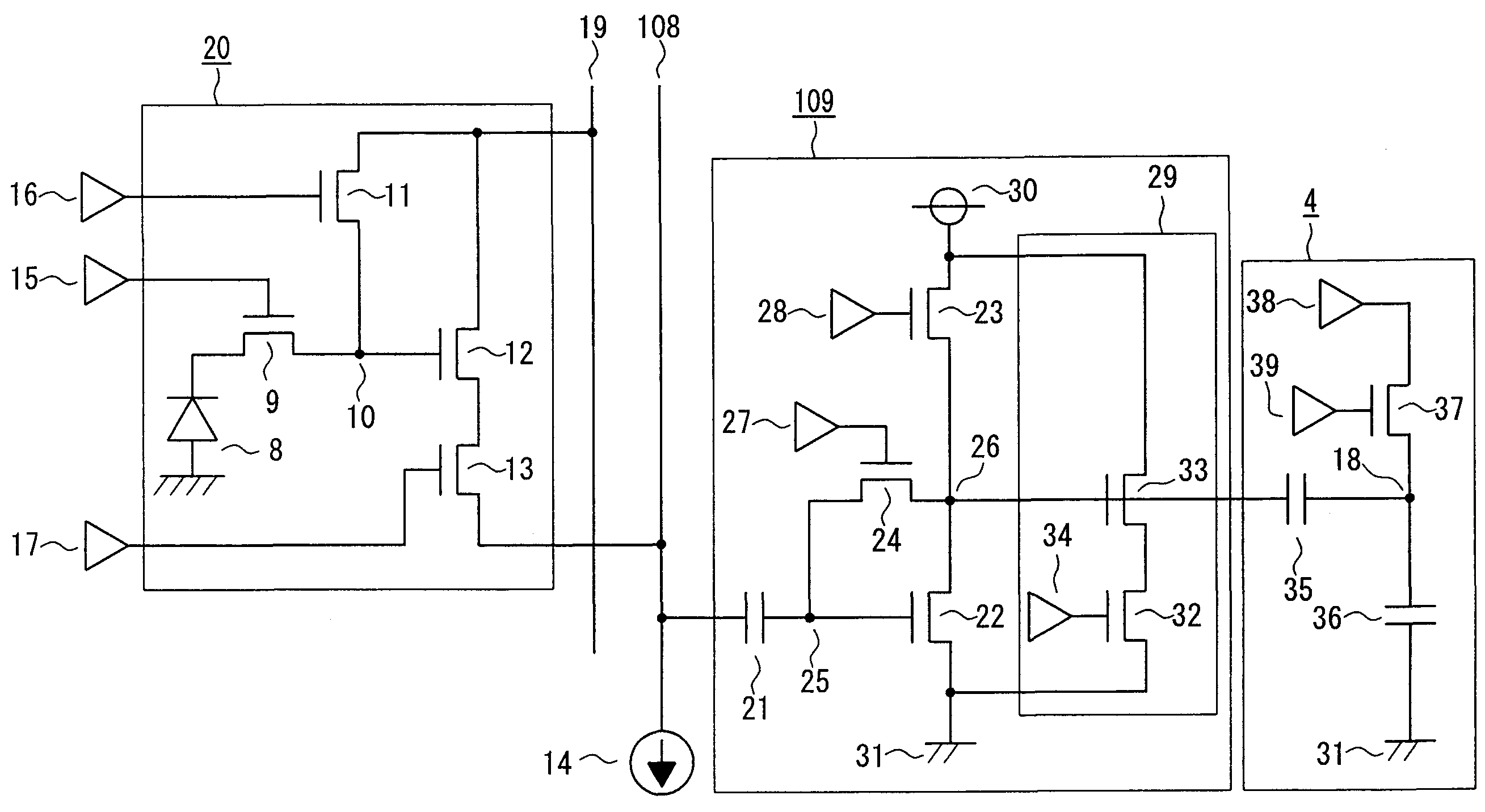
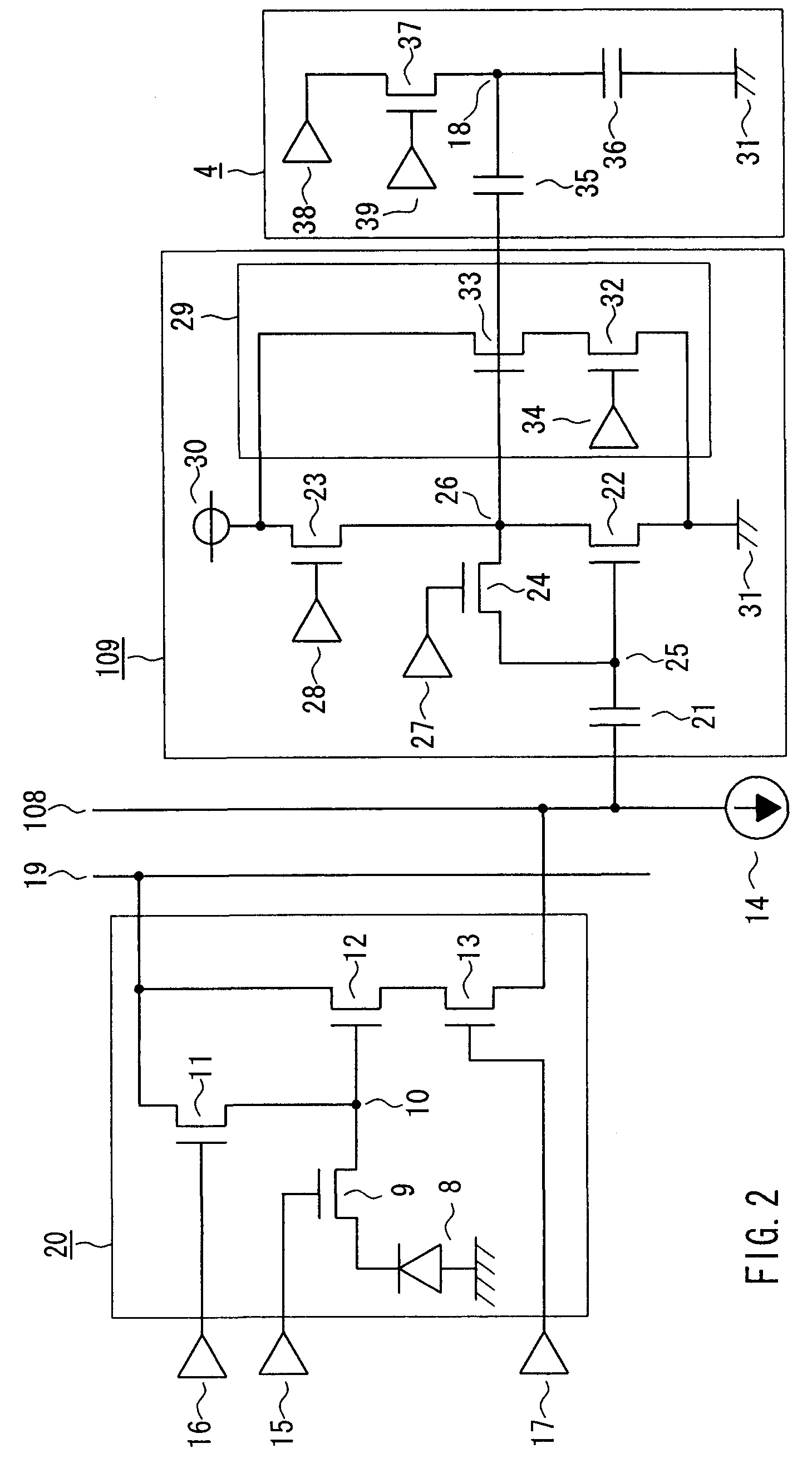
[0038]FIG. 2 is a block circuit diagram specifically showing respective configurations of an i...

second embodiment

[0053]Next, a second embodiment of the solid-state imaging device according to the present invention will be described with reference to the appended drawings. FIG. 6 is a circuit diagram showing a column amplifier 109 and a noise canceling circuit 4 among components in a column circuit portion of a solid-state imaging device according to the second embodiment of the present invention. The configuration shown herein is the same as that of the above-described first embodiment shown in FIG. 2 except for a portion of a current generating circuit 29, and an operation of reading out a pixel signal also is similar to that in the above-described first embodiment. Hence, duplicate descriptions thereof are omitted.

[0054]The current generating circuit 29 includes a first adjustment transistor 32, a second adjustment transistor 33, a reset transistor 40, and a judgment transistor 42. The first adjustment transistor 32 and the second adjustment transistor 33 are connected serially between a col...

third embodiment

[0061]In the following, a third embodiment of the solid-state imaging device according to the present invention will be described with reference to the appended drawings. FIG. 8 is a circuit diagram showing a column amplifier 109 and a noise canceling circuit 4 among components in a column circuit portion of a solid-state imaging device according to the third embodiment of the present invention. As in the second embodiment, the configuration of this embodiment is the same as that of the solid-state imaging element according to the first embodiment shown in FIG. 2 except for a portion of a current generating circuit 29, and an operation of reading out a pixel signal also is similar to that in the first embodiment. Hence, duplicate descriptions thereof are omitted herein.

[0062]In this embodiment, the current generating circuit 29 includes only a first adjustment transistor 32 and not a second adjustment transistor. Because of this, a constant electric current that is determined by a l...


PUM


Abstract

It is an object to obtain a solid-state imaging device that can reduce a variation in an electric current that flows between an amplifier power supply and ground wiring in a column amplifier, which occurs in accordance with an input signal level, without degrading manufacture and operation tolerances in terms of photoelectric conversion characteristics of the solid-state imaging device. A solid-state imaging device includes: a pixel array in which imaging pixels are arranged in row and column directions; a plurality of vertical signal lines, each of which commonly outputs signals from part of the imaging pixels that is aligned in each column of the pixel array; and a plurality of column amplifiers that are provided in a one-to-one correspondence with the plurality of vertical signals lines. In the solid-state imaging device, between a column amplifier power supply and a ground in each of the plurality of column amplifiers, a current generating circuit is provided that generates a correction current in such a direction as to cancel out a variation in an operation current of each of the plurality of column amplifiers.

Description

BACKGROUND OF THE INVENTION[0001]1. Field of the Invention[0002]The present invention relates to a solid-state imaging device, and particularly relates to a solid-state imaging device that can provide high quality images even when capturing an image of a subject with high brightness, and allows large tolerances in manufacture and operational conditions.[0003]2. Description of Related Art[0004]In a MOS type solid-state imaging device, for reading out image signals from a pixel array in which imaging pixels are arranged in a matrix form, generally, an analog memory is provided in each column, and signals are read out from the imaging pixels on a row-by-row basis, and then, the signals kept in the column memories are outputted serially to the outside. Further, it often has been the case with a conventional example of a MOS type solid-state imaging device that a column amplifier is inserted between a pixel array and a column memory. The reason for this is that in a serial readout portio...

Claims


Application Information

Patent Timeline
Patent Type & Authority Applications(United States)
IPC IPC(8): H01L27/146H04N5/335H04N5/357H04N5/369H04N5/374H04N5/376
CPCH04N3/155H04N5/3658H04N5/335H04N25/677H04N25/75H04N25/76H04N25/00
Inventor HARA, KUNIHIKOKUBO, HIROSHI
Owner COLLABO INNOVATIONS INC
Why Eureka
Try Eureka