Optically enhanced multi-spectral detector structure

a detector structure and optical enhancement technology, applied in the direction of optical radiation measurement, instruments, light radiation electric generators, etc., can solve the problems of insufficient materials and processes used to achieve this efficiency, high material cost, and insufficient efficiency per area, etc., to achieve the effect of improving efficiency

Inactive Publication Date: 2008-02-28
EASTMAN KODAK CO
View PDF14 Cites 126 Cited by
  • Summary
  • Abstract
  • Description
  • Claims
  • Application Information

AI Technical Summary

Benefits of technology

[0034]wherein said optical concentrator, said spectral splitting assembly, and said array of optical detector sites are replicated in an array-like fashion to form said integrated optical detector assembly. The optical concentrator, spectral splitting

Problems solved by technology

This can be achieved by various means; however, the cost of the material tends to be higher as the impurities are removed.
While these devices are less expensive that the traditional bulk crystalline materials, they also do not absorb as much incident radiation due to the layer thickness, and therefore, have lower efficiency per area.
The materials and processes utilized to achieve this efficiency are sufficiently expensive, that large area devices may not be economically practical.
While this may be very efficient it does not provide for an inexpensive web or sheet based method of mass-producing solar arrays.
While this concept particularly offers potential improvements in illumination uniformity to the receivers (detectors), the design lacks specific features useful to thin film type solar cells specifically, or for solar cells with a limited spectral bandwidth, more generally.
However, presently the efficiency of these low cost cells is still low and a significant increase is needed.
However, the dyes in these cells can suffer from degradation under heat and UV light, and the cell casing is difficult to seal due to the solvents used in the assembly process.
As solar cells are made thinner, either to reduce the quantity and cost of silicon employed, or to enable thin film solar detection structures, the maximum thickness of the absorbing layers may be limited.
While the optical met

Method used


Image

  • Optically enhanced multi-spectral detector structure
  • Optically enhanced multi-spectral detector structure
  • Optically enhanced multi-spectral detector structure

Examples


Embodiment Construction

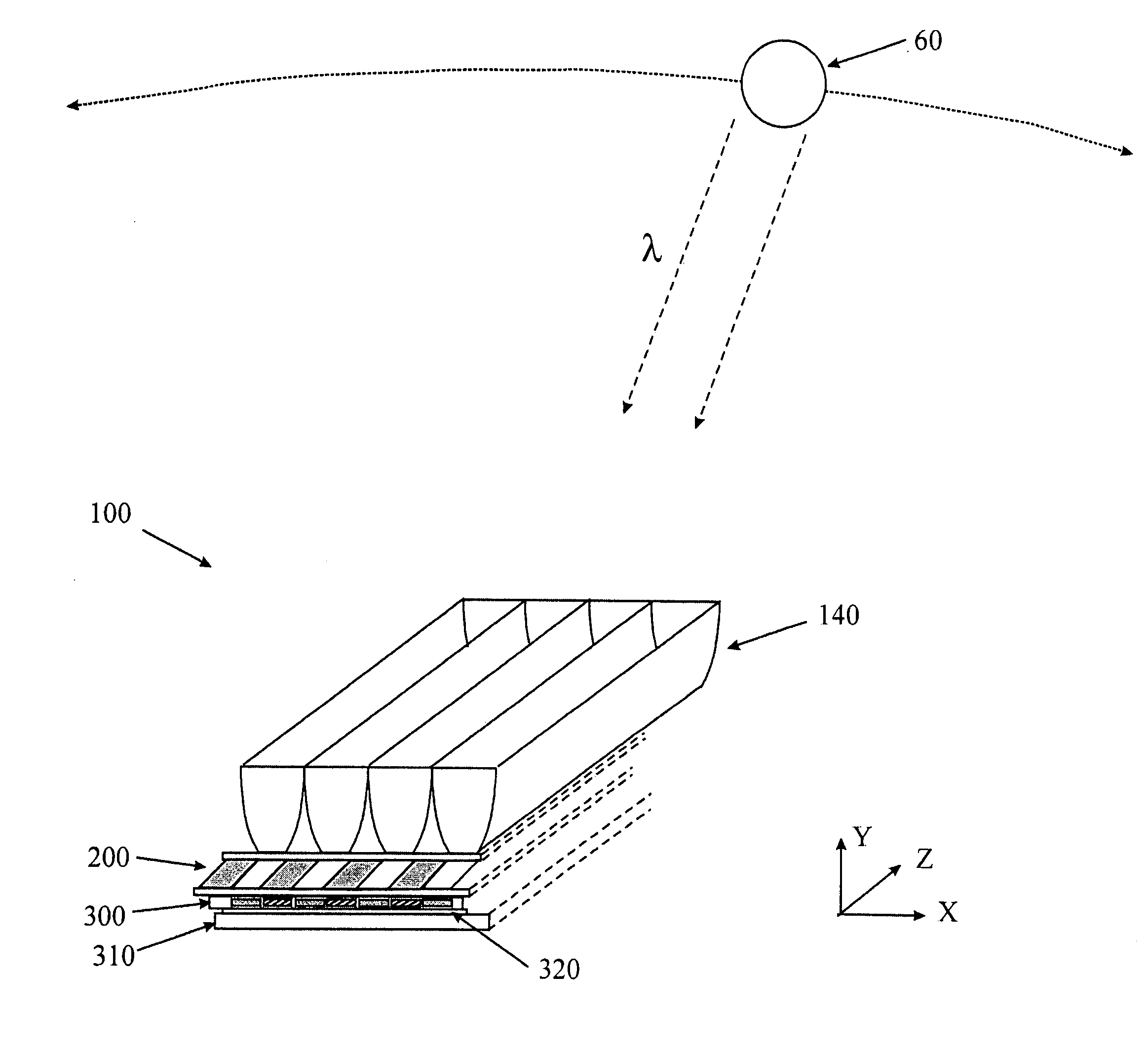
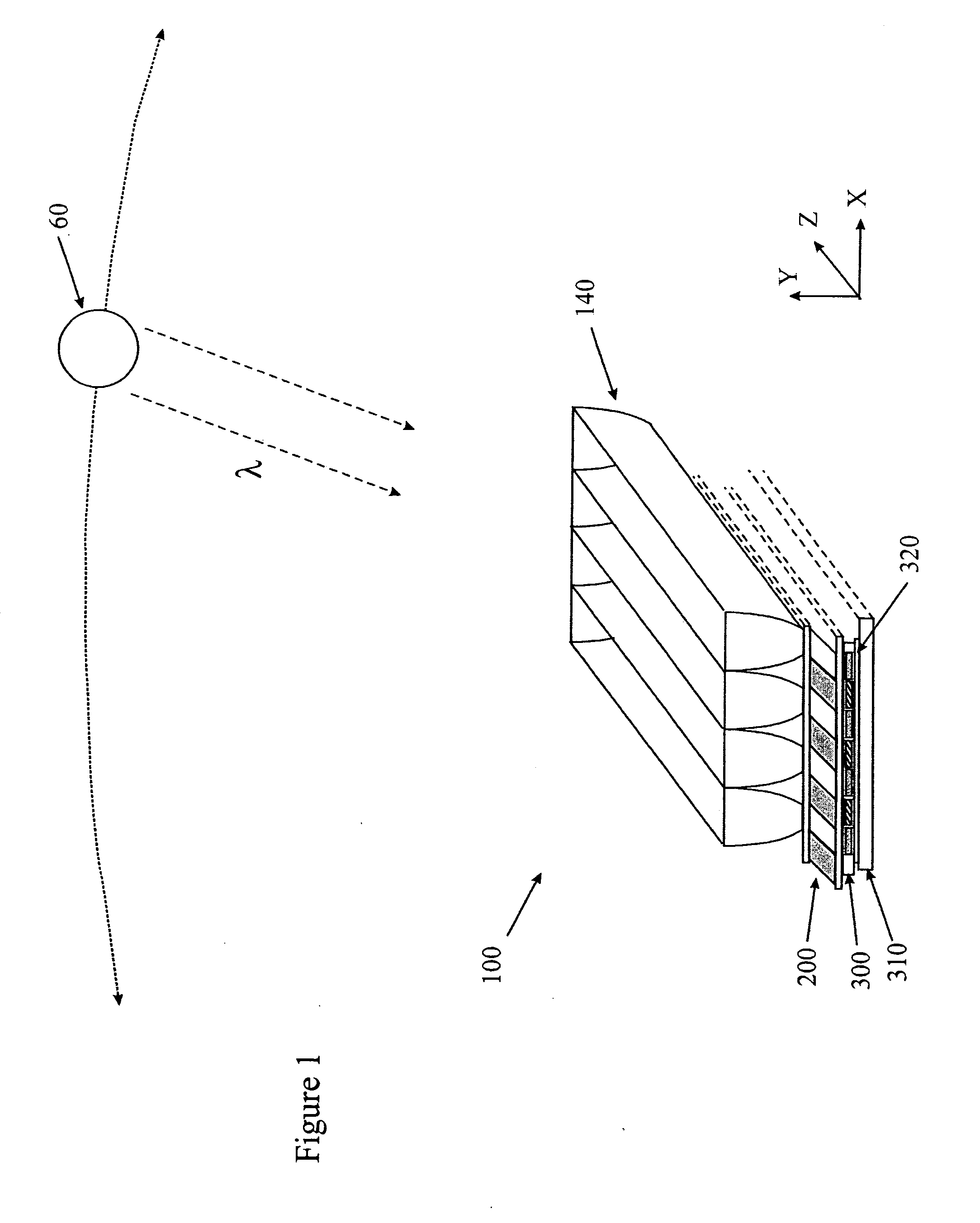
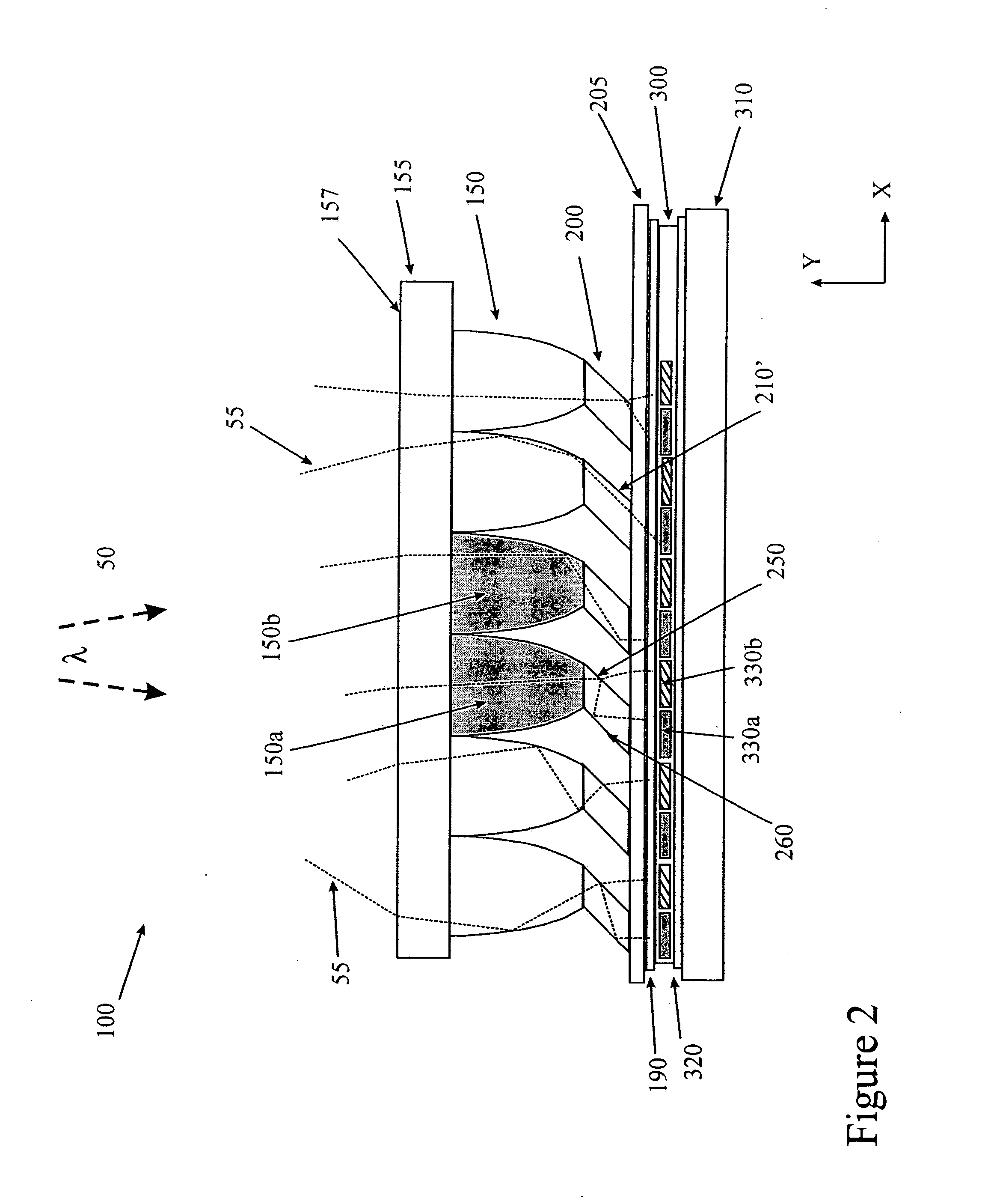
[0047]Classical solar energy conversion uses concentrators, such as CPCs, to maximize the solar power density into the smallest area. In the case of photovoltaic conversion, the historical limits of semiconductor wafer size and cost motivated a maximization of solar energy conversion per unit area. Additionally, as the current produced by photovoltaic cells is proportional to the irradiation incident onto the cells, more light will increase the electrical output. In the case of photo thermal conversion, such as applying solar energy to heat water flowing in a pipe, maximizing solar energy density minimizes the thermal mass and thermal dissipation. Concentrators, such as CPCs, also have a significant additional advantage that the wide acceptance angle, for example ±40°, enabled an efficient solar light conversion that does not require solar tracking. However, in the future, as large area solar cells become increasingly economical, maximum solar concentration may become a less compell...


PUM


Abstract

An integrated optical system and method employs an optical concentrator, a spectral splitting assembly for splitting incident light into multiple beams of light, each with a different nominal spectral bandwidth; and an array of optical detector sites wherein each of the detector sites has a nominal spectral response and wherein the detector sites are spatially arranged to provide an arrangement of said detector sites which are spatially variant relative to said nominal spectral responses. Such a system can be used for purposes such as optical detection and solar collection to provide improved efficiency. Improved efficiency of collection and manufacture are obtainable with using such devices.

Description

CROSS REFERENCE TO RELATED APPLICATIONS[0001]Reference is made to commonly-assigned co-pending U.S. patent application Ser. No. 10 / 702,162 by C. Rider, filed Nov. 5, 2003, and entitled “Photovoltaic Device and a Manufacturing Method Thereof”, and to U.S. patent application Ser. No. 10 / 860,545, filed Jun. 3, 2004, entitled Brightness Enhancement Film using a Linear Arrangement of Light Concentrators, by J. Lee et al., and to U.S. patent application Ser. No. 11 / 247,509 filed Oct. 10, 2005, entitled Backlight Unit with Linearly Reduced Divergence, by J. Lee, the disclosures of which are incorporated herein.FIELD OF THE INVENTION[0002]This invention relates in general to an integrated optical detector assembly designed to receive input light with a wide angular acceptance and multi-spectral band responsiveness. In particular, the invention relates to an optical detector assembly that provides a sheet-like construction, and which may be particularly suitable for solar energy collection.B...

Claims


Application Information

Patent Timeline
IPC IPC(8): G01J3/50H02N6/00
CPCH01L31/0232H01L31/0547Y02E10/52H01L31/02325H01L31/055
Inventor KURTZ, ANDREW F.SILVERSTEIN, BARRY D.
Owner EASTMAN KODAK CO
Why Eureka
Try Eureka