Sensor Circuit, Semiconductor Device, and Electronic Apparatus

Inactive Publication Date: 2008-02-28
ROHM CO LTD
View PDF11 Cites 43 Cited by
  • Summary
  • Abstract
  • Description
  • Claims
  • Application Information

AI Technical Summary

Benefits of technology

[0021] In view of the conventionally experienced problems described above, an object of the present invention is to provide sensor circuits that have a simple structure composed of a minimal number of terminals and that can reduce the curre

Problems solved by technology

In ideal conditions, it can be expected that the magnetic field sensor disclosed in Patent Document 1 performs offset cancellation accurately; in reality, however, the capacitor 4 and the voltage amplifier 3 do not form a perfect differential configuration.
Thus, there is a possibility that, for example, a delay (retardation) caused by the capacitor 4 or ripples or noise in the power supply voltage makes it impossible to adequately perform offset cancellation.
O

Method used


Image

  • Sensor Circuit, Semiconductor Device, and Electronic Apparatus
  • Sensor Circuit, Semiconductor Device, and Electronic Apparatus
  • Sensor Circuit, Semiconductor Device, and Electronic Apparatus

Examples


Example

First Embodiment

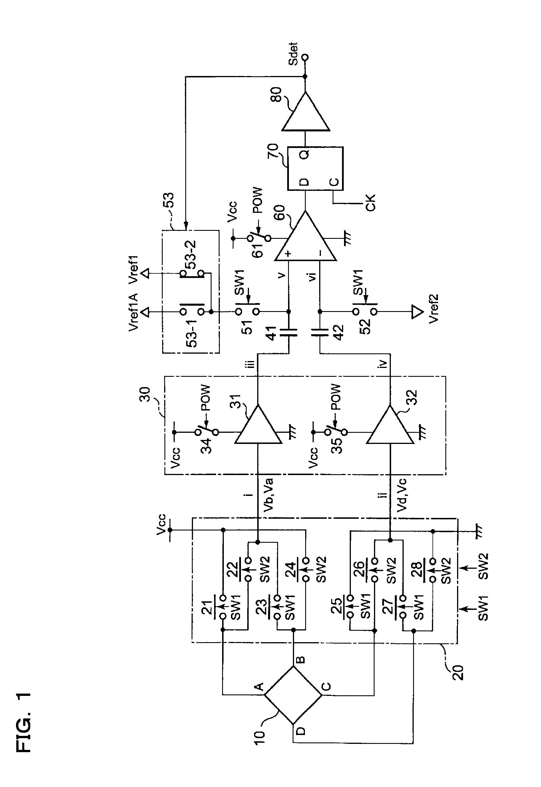
[0046]FIG. 1 is a diagram showing the configuration of a magnetic sensor circuit according to a first embodiment of the invention. This magnetic sensor circuit is disclosed in Japanese Patent Application No. 2005-230781 (claiming priority based on Japanese Patent Application No. 2005-031715), which the applicant of the present invention once filed. In FIG. 1, as is the case with a conventional Hall device shown in FIG. 21, a Hall device 10 is formed in the shape of a plate that is geometrically equivalent with respect to four terminals A, C, B, and D.

[0047] For an effective signal component commensurate with the strength of a magnetic field applied to the Hall device 10, a Hall voltage appearing between a second terminal pair B-D when a power supply voltage Vcc is applied between a first terminal pair A-C of the Hall device 10 is in phase with a Hall voltage appearing between the first terminal pair C-A when the power supply voltage Vcc is applied between the secon...

Example

Second Embodiment

[0093] Now, a second embodiment will be described, taking up as an example a magnetic sensor circuit that can detect the magnetic field strength irrespective of the direction of a magnetic field relative to a Hall device.

[0094]FIG. 6 is a diagram showing the configuration of a magnetic sensor circuit according to the second embodiment disclosed in Japanese Patent Application No. 2005-230781, which the applicant of the present invention once filed. In FIG. 6, a magnetic sensor circuit 1A differs from the magnetic sensor circuit shown in FIG. 1 in that it further includes a control circuit 100, an OR circuit OR1, a latch circuit 71, and an inverter INV0. In other respects, the magnetic sensor circuit 1A is the same as the magnetic sensor shown in FIG. 1, and therefore overlapping descriptions will not be repeated.

[0095] The control circuit 100 outputs a power-supply ON signal POW, a first switching signal SW1, a second switching signal SW2, a third switching signal...

Example

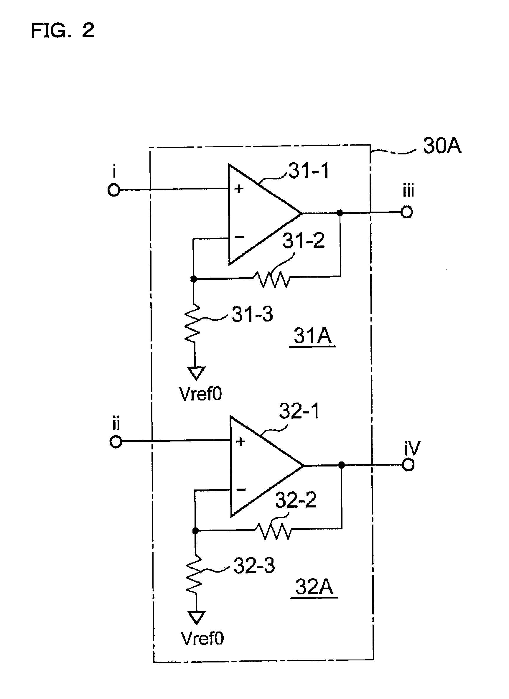
[0138] A third embodiment will be described, taking up as an example a magnetic sensor circuit that can compensate for the temperature characteristic of the sensitivity with which to detect the magnetic field strength. The overall configuration of the magnetic sensor circuit of the third embodiment is the same as that of the magnetic sensor circuit shown in FIG. 1 (or FIG. 6), and therefore overlapping descriptions will not be repeated.

[0139]FIG. 12 is a diagram illustrating a current passing through the Hall device 10 shown in FIG. 1.

[0140] In FIG. 12, the switches 21 and 24 are each composed of a P-channel MOS transistor, and the switches 25 and 28 are each composed of an N-channel MOS transistor. The on resistance of the P-channel MOS transistor is RP, and the on resistance of the N-channel MOS transistor is RN. The resistance of the Hall device 10 is RH. The Hall voltage Vs outputted from the Hall device 10 is given by formula (5) below.

Vs=KH×IH×B   (5)

[0141] Here, KH repres...


PUM


Abstract

A sensor circuit has: a sensor portion that obtains, as an electrical signal, information on an object to be measured or detected; and a control circuit that controls the operation of the sensor portion. The control circuit receives a start input signal inputted thereto from outside for making the sensor portion operate only for a given duration after the start input signal is inputted thereto. With this configuration, it is possible to reduce the current consumption by arbitrarily controlling a period of an intermittent operation of the sensor circuit.

Description

[0001] This application is based on Japanese Patent Application No. 2006-203304 filed on Jul. 26, 2006, the contents of which are hereby incorporated by reference. BACKGROUND OF THE INVENTION [0002] 1. Field of the Invention [0003] The present invention relates to sensor circuits (sensor circuits in general, such as magnetic sensors, temperature sensors, and optical sensors), to semiconductor devices built with such sensor circuits integrated thereinto, and to electronic apparatuses provided with such sensor circuits (for example, portable terminals using battery power supplies). More particularly, the present invention relates to a technology for reducing the electric power consumption of such sensor circuits. [0004] 2. Description of Related Art [0005] In general, a magnetic sensor circuit is composed of a Hall device that outputs an output voltage commensurate with the strength of a magnetic field, an amplifier that amplifies the output voltage of the Hall device, and a comparato...

Claims


Application Information

Patent Timeline
IPC IPC(8): G06F1/32
CPCG01D5/142
Inventor NISHIKAWA, HIDETOSHI
Owner ROHM CO LTD
Why Eureka
Try Eureka