

Method and apparatus for DC offset cancellation in amplifiers
a technology of offset cancellation and amplifier, which is applied in the direction of dc-amplifiers with dc-coupled stages, amplifiers with semiconductor devices/discharge tubes, and differential amplifiers. it can solve the problems of reducing the dynamic range of the transceiver, requiring a method of calibrating the dc offset error, and contributing to the noise at the output of the amplifier
- Summary
- Abstract
- Description
- Claims
- Application Information
AI Technical Summary
Benefits of technology
Problems solved by technology
Method used
Image

Examples
Embodiment Construction
[0027]The embodiments herein and the various features and advantageous details thereof are explained more fully with reference to the non-limiting embodiments that are illustrated in the accompanying drawings and detailed in the following description. Descriptions of well-known components and processing techniques are omitted so as to not unnecessarily obscure the embodiments herein. The examples used herein are intended merely to facilitate an understanding of ways in which the embodiments herein may be practiced and to further enable those of skill in the art to practice the embodiments herein. Accordingly, the examples should not be construed as limiting the scope of the embodiments herein.
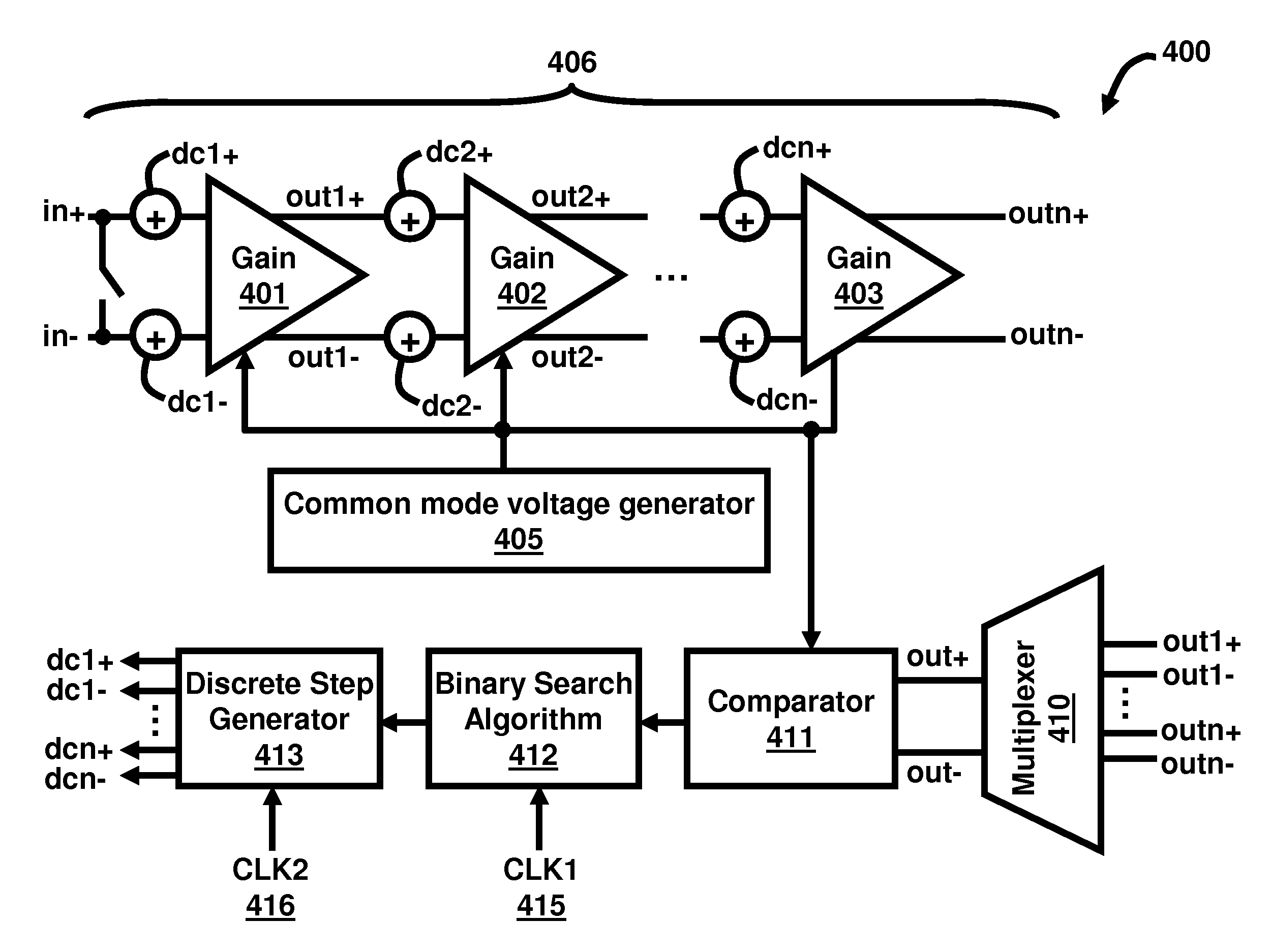
[0028]As mentioned, there remains a need for a digital DC offset error correction technique with high precision, especially in the context of a cascade of amplifiers. The embodiments herein achieve this by providing a technique for canceling undesired DC offsets that are problematic in a high-g...
PUM
 Abstract
Description
Claims
Application Information