Plasma reactor with inductie excitation of plasma and efficient removal of heat from the excitation coil

Active Publication Date: 2008-02-28
MATTSON TECHNOLOGY +1
View PDF49 Cites 33 Cited by
  • Summary
  • Abstract
  • Description
  • Claims
  • Application Information

AI Technical Summary

Benefits of technology

[0017] Deep immersion of the antenna cells having the above-described structure with ferromagnetic core provides high efficiency of plasma excitation, while the arrangement of the plasma

Problems solved by technology

Asymmetry of the RF field results in plasma azimuthal asymmetry and non-uniformity of treatment.
On the other hand, matching of the coil having low inductance with a standard resonance matching network becomes energy inefficient due to extra-large RF current and thus high power losses in the matcher network and in the coil itself.
A common problem that occurs in industrial ICP reactors for plasma processing results from a high RF voltage (a few kV) between the terminals of the inductor coil (antenna).
High antenna RF voltage requires special means for adequate electrical insulation and leads to considerable capacitive coupling between the coil and plasma.
This negative potential accelerates the plasma ions towards the window causing erosion and sputtering of the latter whereby plasma is contaminated.
Another problem inherent in plasma processing ICP sources is a transmission line effect along the coil conductor.
This effect occurs due to capacitive coupling of the induction coil to plasma and/or to grounded parts of the plasma reactor, resulting in the coil current non-uniformity along the coil wire, thus leading to the plasma azimuthal non-uniformity.
The transmission line effect is an increasing problem for large RF plasma reactors when the coil wire length becomes comparable to the wavelength of the working f

Method used


Image

  • Plasma reactor with inductie excitation of plasma and efficient removal of heat from the excitation coil
  • Plasma reactor with inductie excitation of plasma and efficient removal of heat from the excitation coil
  • Plasma reactor with inductie excitation of plasma and efficient removal of heat from the excitation coil

Examples


Example

[0028] The foregoing has outlined, in general, the physical aspects of the invention and is to serve as an aid to better understanding the more complete detailed description which is to follow. In reference to such, there is to be a clear understanding that the present invention is not limited to the method or detail of construction, fabrication, material, or application of use described and illustrated herein. Any other variation of fabrication, use, or application should be considered apparent as an alternative embodiment of the present invention.

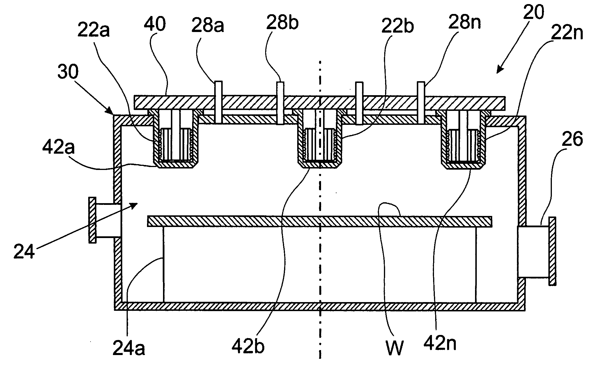
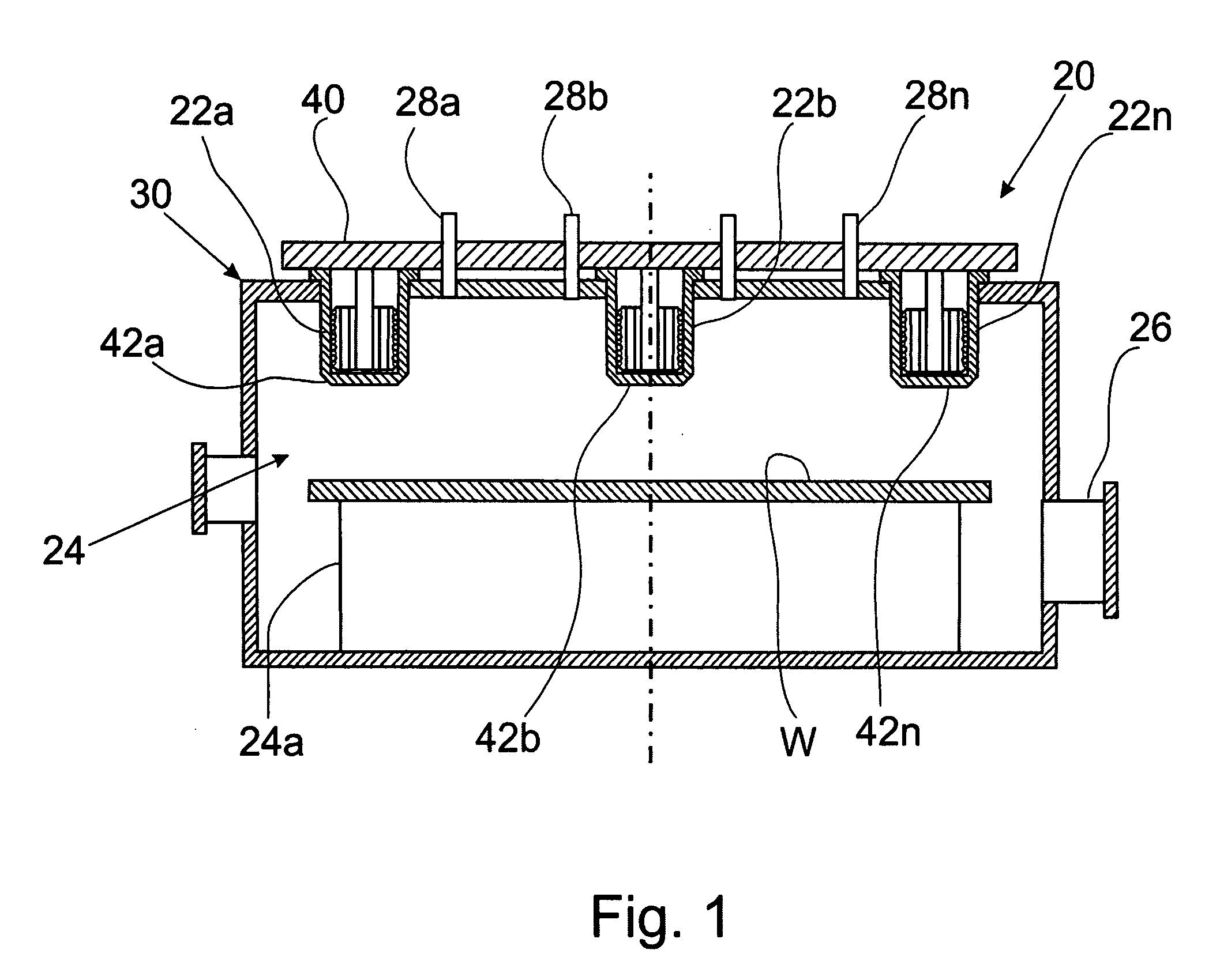
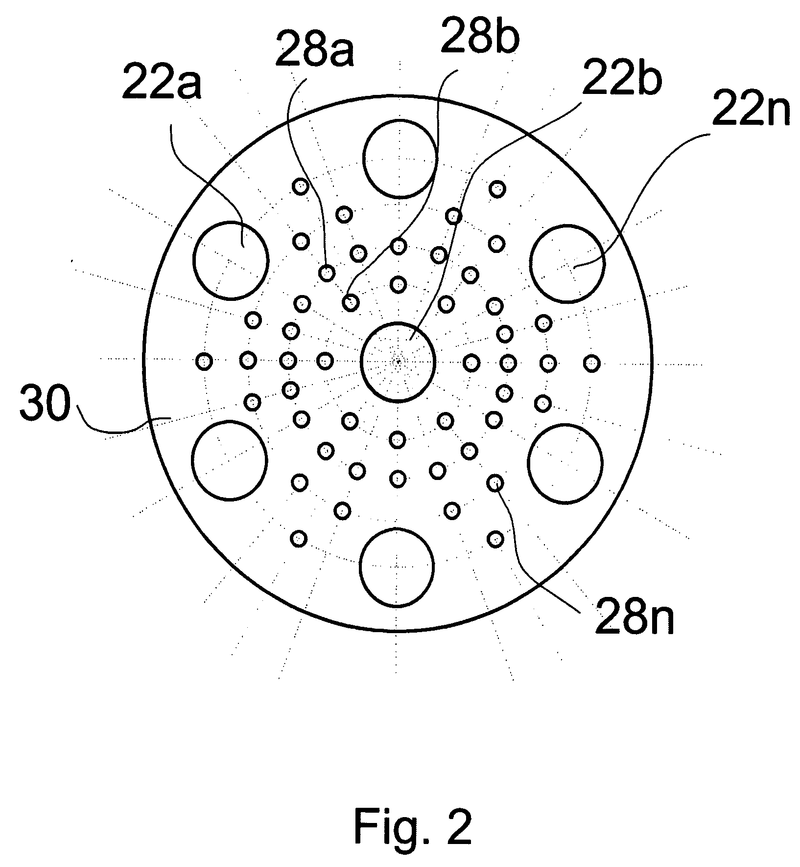
[0029]FIG. 1 is a vertical sectional view of a multiple-cell RF plasma reactor 20 with an array of ferromagnetic RF-antenna cells 22a, 22b, . . . 22n completely immersed into the plasma volume generated in the working chamber 24 of the reactor 20. FIG. 2 is a bottom view of the reactor cover that shows arrangement of individual RF-antenna cells. Reference numeral 26 shows an outlet port 26 connection to a vacuum system (not shown) for ev...


PUM


Abstract

The plasma reactor of the invention is intended for treating the surfaces of objects such as semiconductor wafers and large display panels, or the like, with plasma. The main part of the plasma reactor is an array of RF antenna cells, which are deeply immersed into the interior of the working chamber. Each antenna cell has a ferromagnetic core with a heat conductor and a coil wound onto the core. The core and coil are sealed in the protective cap. Deep immersion of the antenna cells having the structure of the invention provides high efficiency of plasma excitation, while the arrangement of the plasma cells and possibility of their individual adjustment provide high uniformity of plasma distribution and possibility of adjusting plasma parameters, such as plasma density, in a wide range.

Description

FIELD OF THE INVENTION [0001] The present invention is related to a plasma reactor with inductive excitation of plasma for plasma processing of various objects such as semiconductor materials and large panel displays by etching, coating, activating, or otherwise treating surfaces of various parts by means of plasma. The plasma reactor of the invention has advantage of efficient removal of heat from the excitation coil, high energetic efficiency of plasma generation, which is free of capacitive coupling, high power transfer efficiency, and effective plasma uniformity control. BACKGROUND OF THE INVENTION [0002] Inductive plasma reactors, which typically consist of reactor chambers and inductively coupled plasma (ICP) sources, are commonly recognized as advanced, convenient, and cost-effective devices for plasma processing of parts and materials at various stages of large-scale manufacturing, e.g., of semiconductor chips and large panel displays. Such sources are also used for activati...

Claims


Application Information

Patent Timeline
IPC IPC(8): B01J19/12
CPCH01J37/321H05H1/46H01J37/32724H01J37/3255H01J37/3211H01J37/32183H01J37/32458H01J2237/332H01J2237/334H01J2237/338
Inventor GODYAK, VALERY
Owner MATTSON TECHNOLOGY
Why Eureka
Try Eureka