Semiconductor device

a technology of semiconductor devices and semiconductors, applied in the direction of semiconductor devices, basic electric elements, electrical equipment, etc., can solve the problems of reducing the miniaturization limit of on-chip circuit elements, and reducing the length of data retention time. , to achieve the effect of low voltage drivability, large threshold voltage shift, and large storage capacity

Inactive Publication Date: 2008-03-06
TOSHIBA MEMORY CORP
View PDF15 Cites 38 Cited by
  • Summary
  • Abstract
  • Description
  • Claims
  • Application Information

AI Technical Summary

Benefits of technology

[0022]According to this invention, it becomes possible to provide the intended semiconductor device capable of realizing both low-voltage drivability and large storage capacity (miniatur

Problems solved by technology

Unfortunately, flash memories with the floating electrode made of polysilicon suffers from a limit in miniaturization of on-chip circuit elements.
This can be said because the polysilicon floating electrode is difficult in scaling in its lengthwise direction, posing a problem as to unwanted interference between adjacent memory cells occurring due to capacitive coupling therebetween.
This causes a problem as to the difficulty in making the tunnel oxide film thinner by thin-film fabrication processes.
This is because of the fact that if this tunnel insulator film is thin, its current leakage increases, resulting in a decrease in length of the data retention time.
However, simply thickening the charge storage dielectric film and the tunnel insulator film accompanies the risk of an unwanted increase in voltage needed when performing writing bas

Method used


Image

  • Semiconductor device
  • Semiconductor device
  • Semiconductor device

Examples


first embodiment

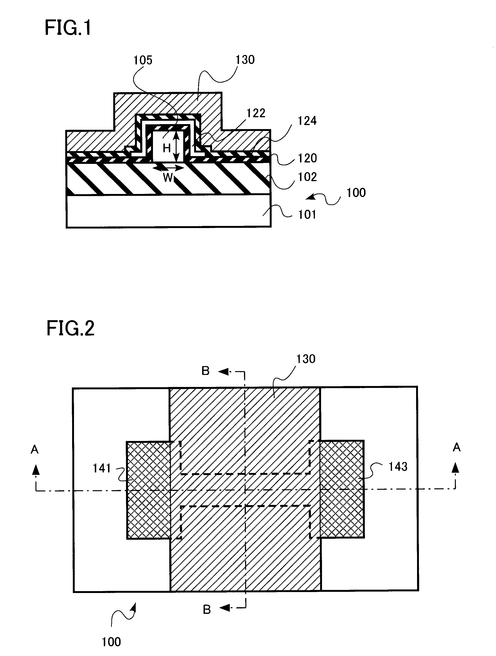
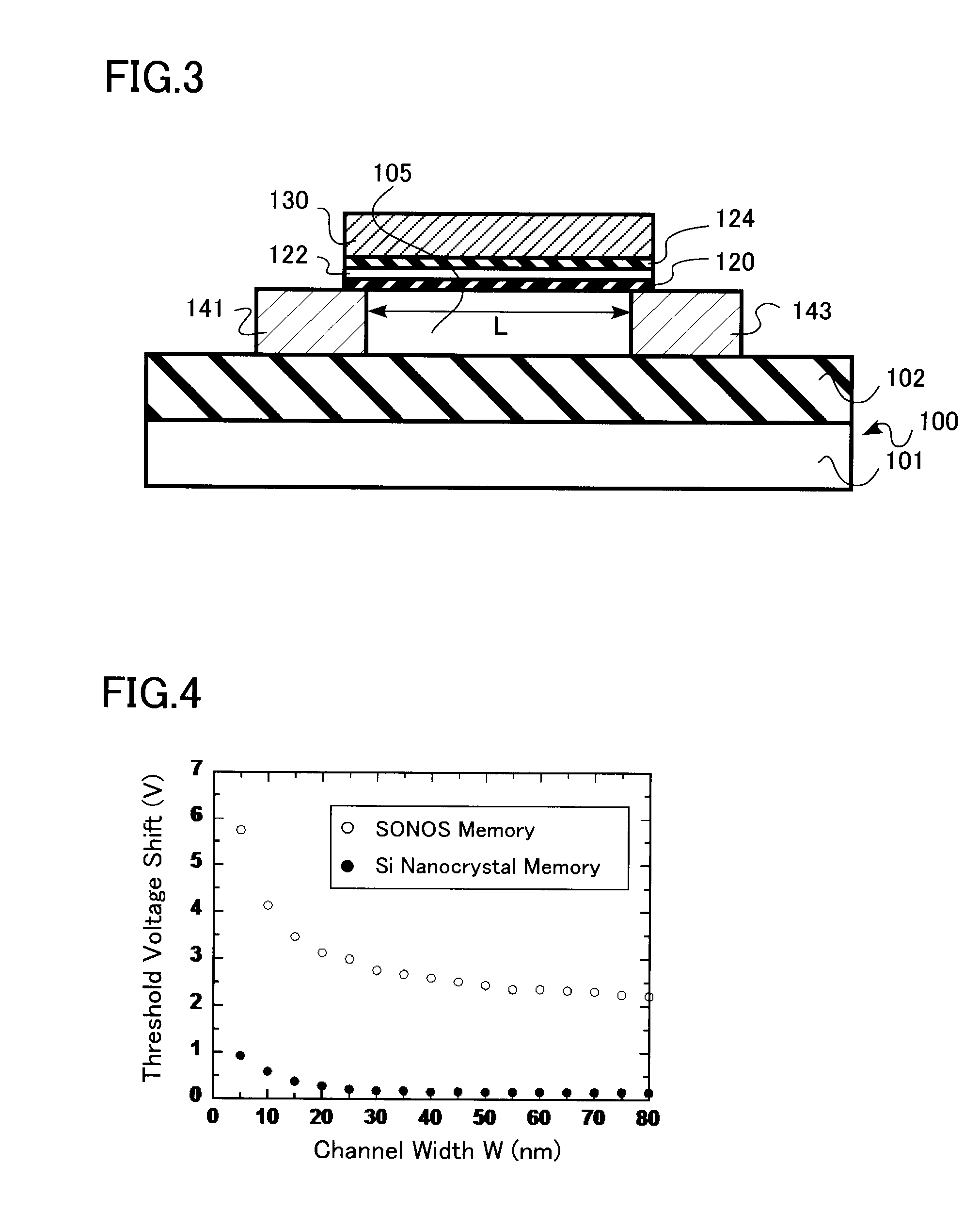
[0048]A semiconductor device having an electrically writable and erasable nonvolatile semiconductor memory (NVSM) circuit element in accordance with one embodiment of this invention is illustrated in FIGS. 1 to 3. A sectional view of the NVSM memory shown in FIG. 1 is taken along line A-A of its upper plan view shown in FIG. 2. Another sectional view of it is shown in FIG. 3 as taken along line B-B of FIG. 2.

[0049]The semiconductor device of the illustrative embodiment is a memory of the silicon-oxide-nitride-oxide-silicon (SONOS) type, which is formed on a semiconductor substrate having a layer of buried dielectric film. This SONOS memory has a channel region with the so-called fine-line type three-dimensional (3D) structure (referred to hereinafter as fine-line SONOS memory). The channel region is arranged so that its width and height are each set to 10 nanometers (nm) or less.

[0050]More specifically, as shown in FIG. 3, the NVSM cell is formed on a silicon (Si) substrate 100. Thi...

second embodiment

[0087]A semiconductor device including a SONOS NVSM cell structure in accordance with another embodiment of this invention is depicted in FIGS. 22 to 24, wherein FIG. 22 shows an upper plan view of the device, FIG. 23 shows a cross-sectional view as taken along line K-K of FIG. 22, and FIG. 24 is a sectional view along line L-L of FIG. 22. This embodiment device is similar to that shown in FIGS. 1-3 with the semiconductor substrate 100 being modified to have no buried dielectric film therein.

[0088]With the NVSM cell-including semiconductor device also embodying the invention, it becomes possible to reduce manufacturing costs by use of such buried dielectric-less substrate—namely, bulk substrate.

third embodiment

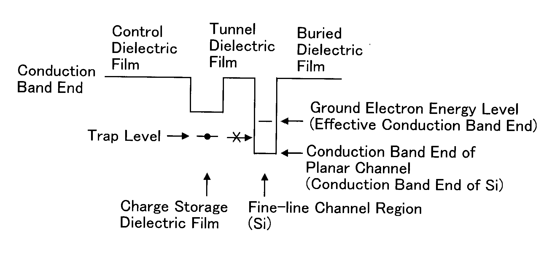
[0089]A semiconductor device having a SONOS NVSM cell in accordance with still another embodiment of this invention is similar to that shown in FIGS. 1-3 with the electron energy level of a trap level in the charge storage insulator film 122 shown in FIG. 1 being arranged to be lower than the energy level at an end of conduction band silicon.

[0090]Arranging the electron energy level at trap level in the charge storage insulator film 122 to be less than or equal to the energy level of silicon's conduction band end is reworded in a way that Et is zero (0) or less with the energy level of silicon conduction band end being as a reference, where Et is the electron energy level of trap level in the charge storage insulator film.

[0091]One possible approach to letting Et be 0 or less is to use as the charge storage insulator film either a hafnium oxide (HfO2) film or a silicon nitride film with enlarged silicon composition (SixNy, where x / y>¾).

[0092]By setting Et to 0 or less as in this emb...


PUM


Abstract

A semiconductor device capable of realizing low-voltage drivability and large storage capacity (miniaturization) by achieving large threshold voltage shifts and long retention time while at the same time suppressing variations in characteristics among memory cells is disclosed. The device includes a semiconductor memory cell having a channel region formed in a semiconductor substrate, a tunnel insulator film on the channel region, a charge storage insulator film on the tunnel insulator film, a control dielectric film on the charge storage film, a control electrode on the control dielectric film, and source/drain regions at opposite ends of the channel region. The memory cell's channel region has a cross-section at right angles to a direction along the channel length, the width W and height H of which are each less than or equal to 10 nm.

Description

CROSS-REFERENCE TO RELATED APPLICATION[0001]This application is based upon and claims the benefit of priority from Japanese Patent Application No. 2006-237306, filed on Sep. 1, 2006, the entire contents of which are incorporated herein by reference.FIELD OF THE INVENTION[0002]This invention relates generally to semiconductor device technologies and, more particularly, to semiconductor devices of the type having a nonvolatile semiconductor memory element.BACKGROUND OF THE INVENTION[0003]An electrically erasable programmable semiconductor storage element capable of retaining data even after power is shut off is called the nonvolatile semiconductor memory (NVSM). NVSM cells of this type are becoming more important for use as storage media in advanced electronics equipment, including handheld or “mobile” information processing tools. Today, these memories are in progress of development for achieving ultra-low voltage drivability and extra-large storage capacity. One of currently major N...

Claims


Application Information

Patent Timeline
IPC IPC(8): H01L29/792
CPCH01L21/845H01L27/115H01L27/11568H01L27/1211H01L29/792H01L29/66795H01L29/66833H01L29/785H01L29/4234H10B69/00H10B43/30
Inventor SAITOH, MASUMIUCHIDA, KEN
Owner TOSHIBA MEMORY CORP
Why Eureka
Try Eureka