Method and apparatus for reducing flicker noise in a semiconductor device

a technology of semiconductor devices and flicker noise, applied in the field of field-effect transistors, can solve the problems of weak increase of flicker noise under hot carrier stress, affecting the surface roughness, and affecting the growth rate of low-quality native oxides relatively quickly

Inactive Publication Date: 2008-03-06
INFINEON TECH AG
View PDF22 Cites 39 Cited by
  • Summary
  • Abstract
  • Description
  • Claims
  • Application Information

AI Technical Summary

Problems solved by technology

Another effect that influences flicker noise is surface roughness.
The lower binding energy of H2 compared to fluorine leads to stronger increase of flicker noise under hot carrier stress.
Low-quality native oxide grows relatively quick and is a problem in achieving very thin high-quality gate oxides.
Smaller thicknesses could lead to higher gate leakage currents and larger thicknesses could require gate voltages above 5 V. Neither of these scenarios are desirable and hence not used in battery-driven systems.
Flicker noise is a design constraint that limits complimentary metal oxide semiconductor (CMOS) RF and analog circuit performance with respect to signal-to-noise ratio in low-noise amplifiers (LNA), noise contribution of direct down conversion mixers and phase noise of voltage-controlled oscillators (VCO).
In some embodiments, metal gates provide low diffusivity towards dopants such as fluorine and consequently implantation of fluorine into gate insulators is prohibited using conventional meth...

Method used


Image

  • Method and apparatus for reducing flicker noise in a semiconductor device
  • Method and apparatus for reducing flicker noise in a semiconductor device
  • Method and apparatus for reducing flicker noise in a semiconductor device

Examples


Embodiment Construction

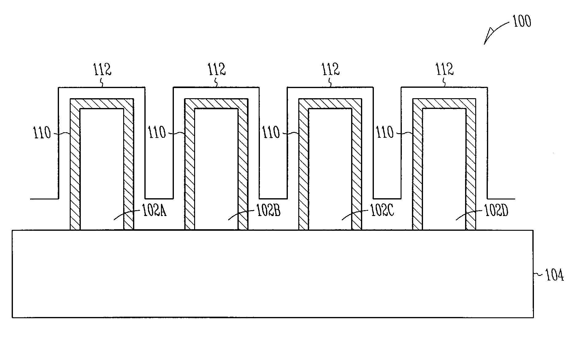
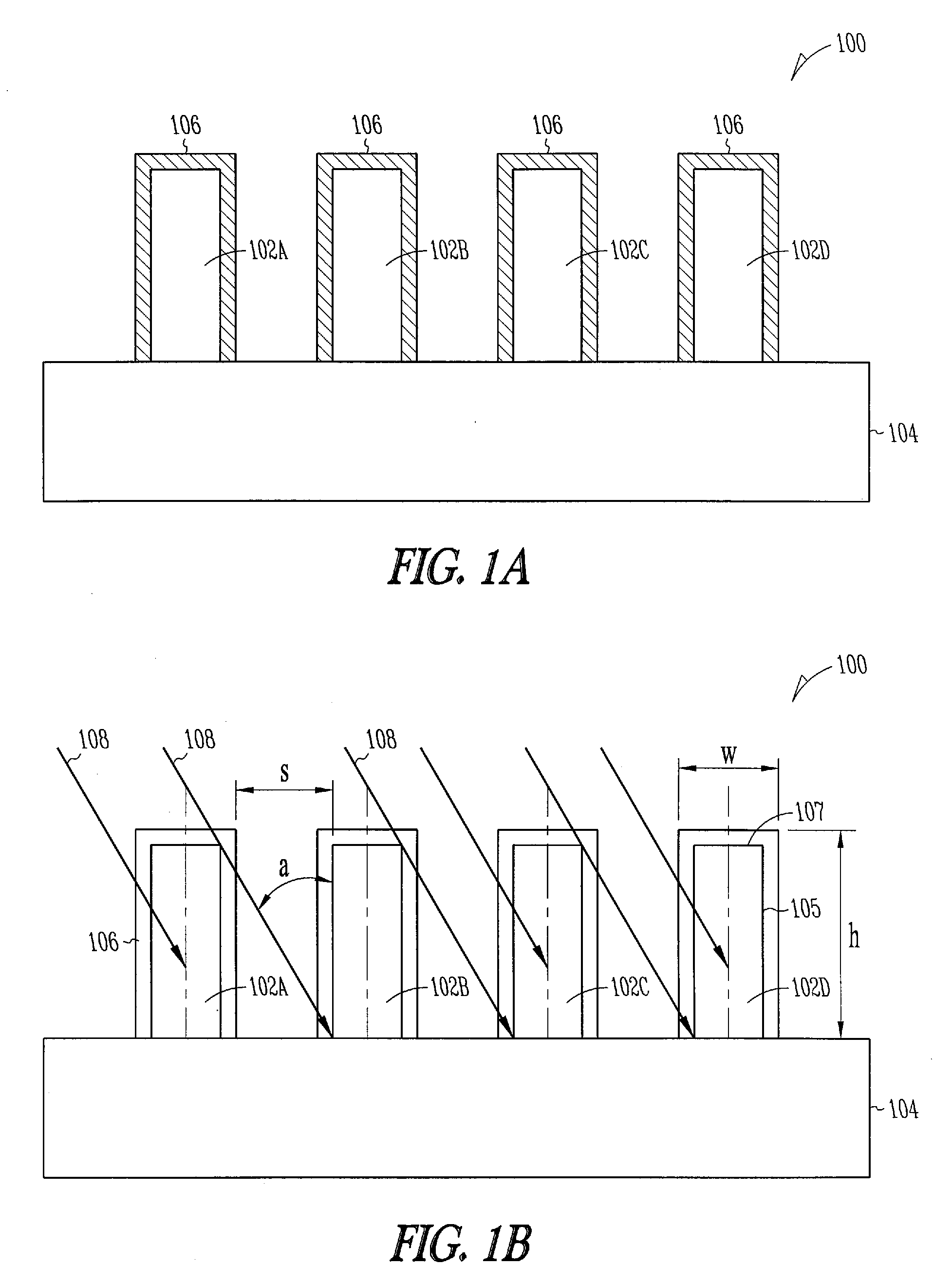
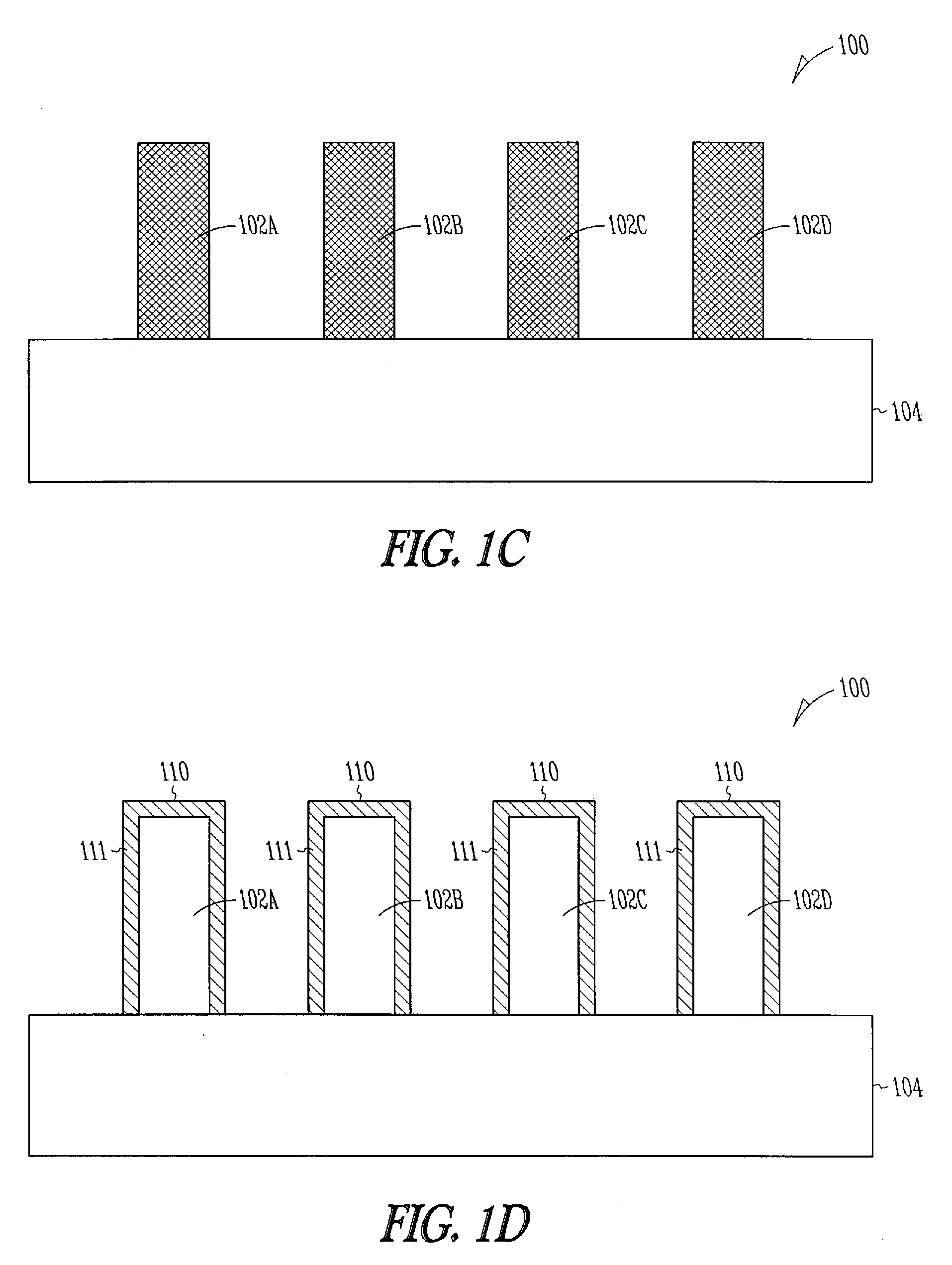
[0007]The following detailed description refers to the accompanying drawings that show, by way of illustration, specific details and embodiments in which the invention may be practiced. These embodiments are described in sufficient detail to enable those skilled in the art to practice the invention. Other embodiments may be utilized and structural, logical, and electrical changes may be made without departing from the scope of the invention. The various embodiments are not necessarily mutually exclusive, as some embodiments can be combined with one or more other embodiments to form new embodiments.

[0008]In the following description, the terms “wafer” and “substrate” may be used interchangeably to refer generally to any structure on which integrated circuits are formed and also to such structures during various stages of integrated circuit fabrication. The term “substrate” is understood to include a semiconductor wafer. The term “substrate” is also used to refer to semiconductor stru...


PUM


Abstract

Some embodiments discussed relate to an integrated circuit and methods for making it, comprises a semiconductor substrate and a plurality of fins disposed on the semiconductor substrate and a gate insulator disposed on the plurality of fins and a gate stack disposed on the gate insulator and the plurality of fins are implanted by a dopant.

Description

RELATED APPLICATIONS[0001]This patent application claims the benefit of priority, under 35 U.S.C. Section 119(e), to U.S. Provisional Patent Application No. 60 / 813,630, filed on Aug. 30, 2006, which is incorporated herein by reference.TECHNICAL FIELD[0002]Embodiments described herein relate generally to semiconductor devices and more particularly, to field-effect transistors (FETs) and methods of fabricating the same.BACKGROUND[0003]Flicker noise is a dominant noise source in metal oxide semiconductor field-effect transistor (MOSFET) devices at low frequencies. In battery-driven circuits where signal-to-noise ratio cannot be improved at the cost of power consumption, a reduction of flicker noise is desired.BRIEF DESCRIPTION OF THE DRAWINGS[0004]FIG. 1A-1E illustrate a sequence of cross-sectional drawings of a partially completed semiconductor wafer showing some embodiments of a method of fabrication of a semiconductor device having a dopant implanted into silicon fins.[0005]FIG. 2 i...

Claims


Application Information

Patent Timeline
IPC IPC(8): H01L29/78H01L21/336
CPCH01L21/845H01L27/1211H01L29/7854H01L29/785H01L29/7851H01L29/66803
Inventor SIPRAK, DOMAGOJ
Owner INFINEON TECH AG
Why Eureka
Try Eureka