Nitride semiconductor laser element and method for manufacturing same

a laser element and semiconductor technology, applied in semiconductor lasers, lasers, semiconductor/solid-state device details, etc., can solve the problems of increased substrate diameter, low manufacturing yield, and difficult manufacturing of uniform overall substrates in the form of wafers, so as to suppress the generation of tensile strain

Inactive Publication Date: 2008-03-06
NICHIA CORP
View PDF5 Cites 17 Cited by
  • Summary
  • Abstract
  • Description
  • Claims
  • Application Information

AI Technical Summary

Benefits of technology

[0016]The present invention is conceived in an effort to solve the above problems. As a specific example, it is an object of the present invention to provide a nitride semiconductor laser element in which a nitride semiconductor layer is grown on a nitride semiconductor substrate having high dislocation density regions and low dislocation density regions, wherein the propagation of dislocations from the high dislocation density region to the drive (main light emission) region of the nitride semiconductor layer, and the generation of tensile strain can be suppressed, and to provide a method for manufacturing this element.

Problems solved by technology

Low manufacturing yield is generally a problem with nitride semiconductor laser elements, and the substrate is one of the reasons for this.
A GaN substrate is different from a GaAs substrate or InP substrate in that manufacturing a low-dislocation substrate that is uniform overall in the form of a wafer is difficult.
And even if a low-dislocation substrate can be manufactured, a new problem is the increased diameter of the substrate.
This poses the risk of adversely affecting the characteristics of the drive (main light emission) region of the nitride semiconductor layer.
Also, since the lattice constants do not match perfectly between the GaN substrate and the nitride semiconductor layer, tensile strain is produced in the nitride semiconductor layer.
This tensile strain creates cracks within the wafer, which lower the yield of the product.
However, with JP-2004-327879-A, since the recesses are formed after the nitride semiconductor layer has been grown on the nitride semiconductor substrate, any dislocations (defects) that occurred at the stage of growing the nitride semiconductor layer, and particularly any dislocations that have propagated to the laser waveguide region, cannot be eliminated.
Also, growing the nitride semiconductor layer over a nitride semiconductor substrate that includes dislocations makes tensile strain more likely to occur, so cracks are more prone to develop.
Furthermore, tensile strain is produced by etching, growing the nitride semiconductor layer, and so forth in subsequent device steps, and this is another source of new cracks.
With JP-2005-294416-A, merely forming recesses in the high dislocation density region can prevent the reoccurrence of dislocations, but it can not adequately suppress cracking, therefore producing nitride semiconductor laser elements at a stable yield cannot be expected.

Method used


Image

  • Nitride semiconductor laser element and method for manufacturing same
  • Nitride semiconductor laser element and method for manufacturing same
  • Nitride semiconductor laser element and method for manufacturing same

Examples


embodiment 1

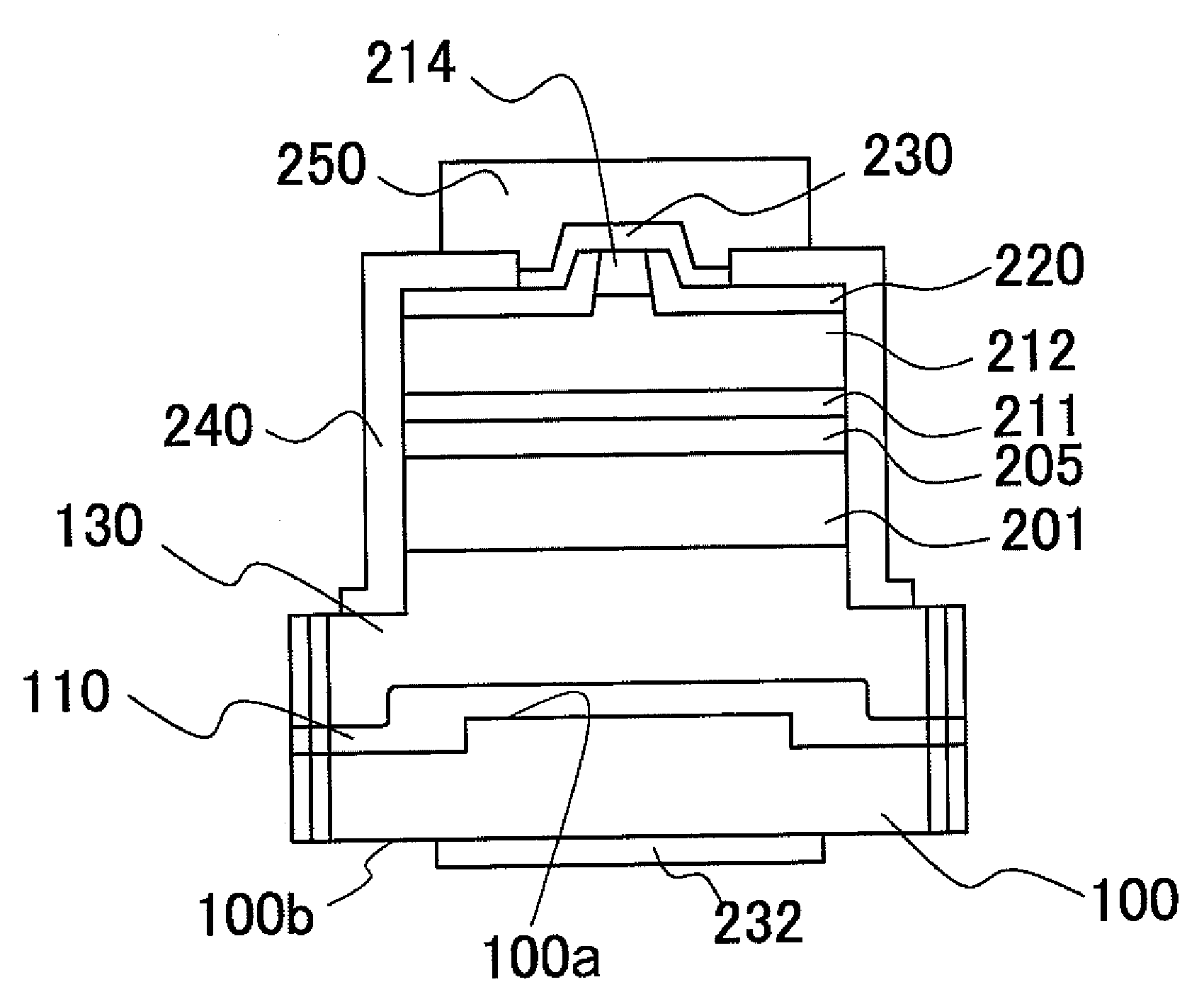
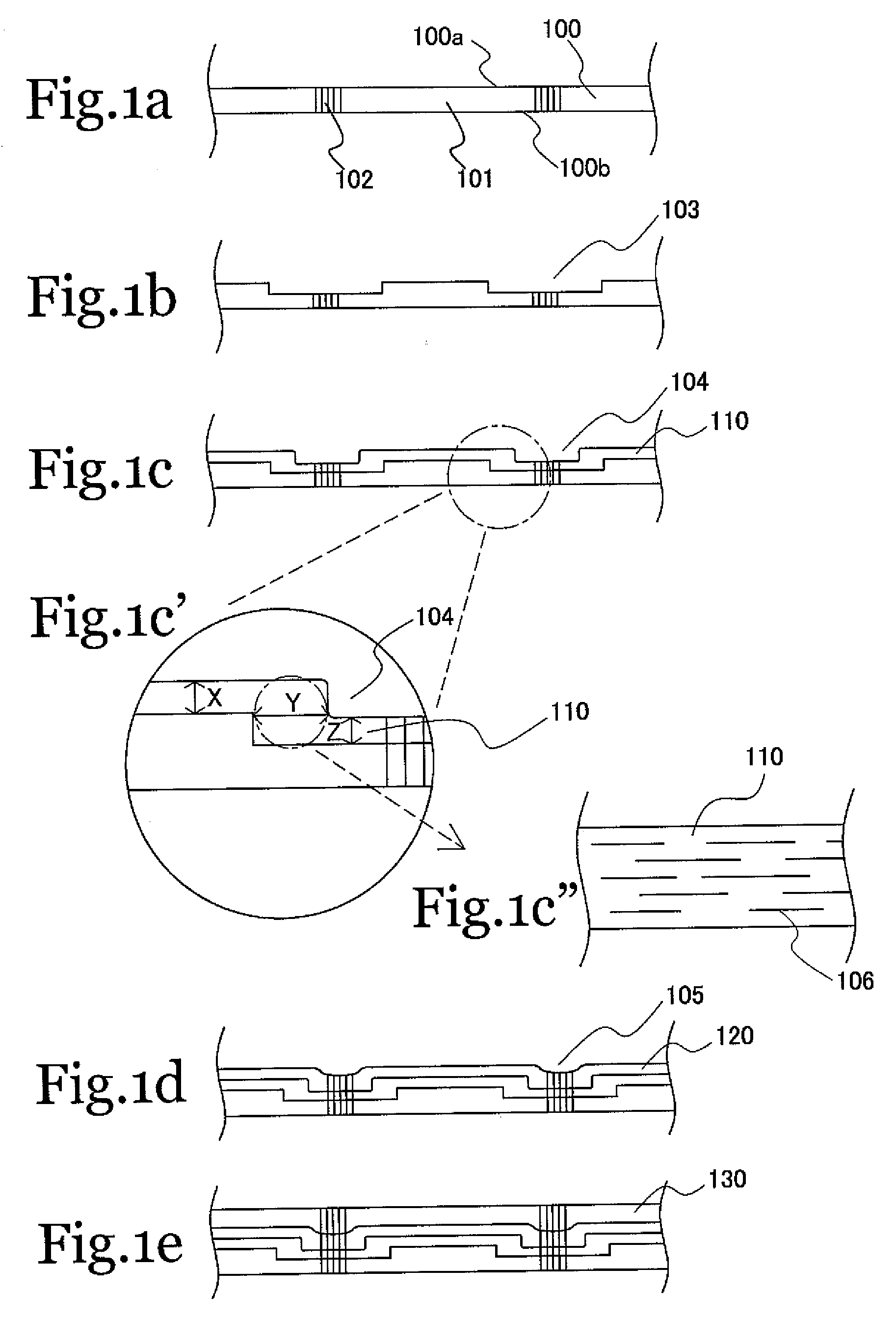
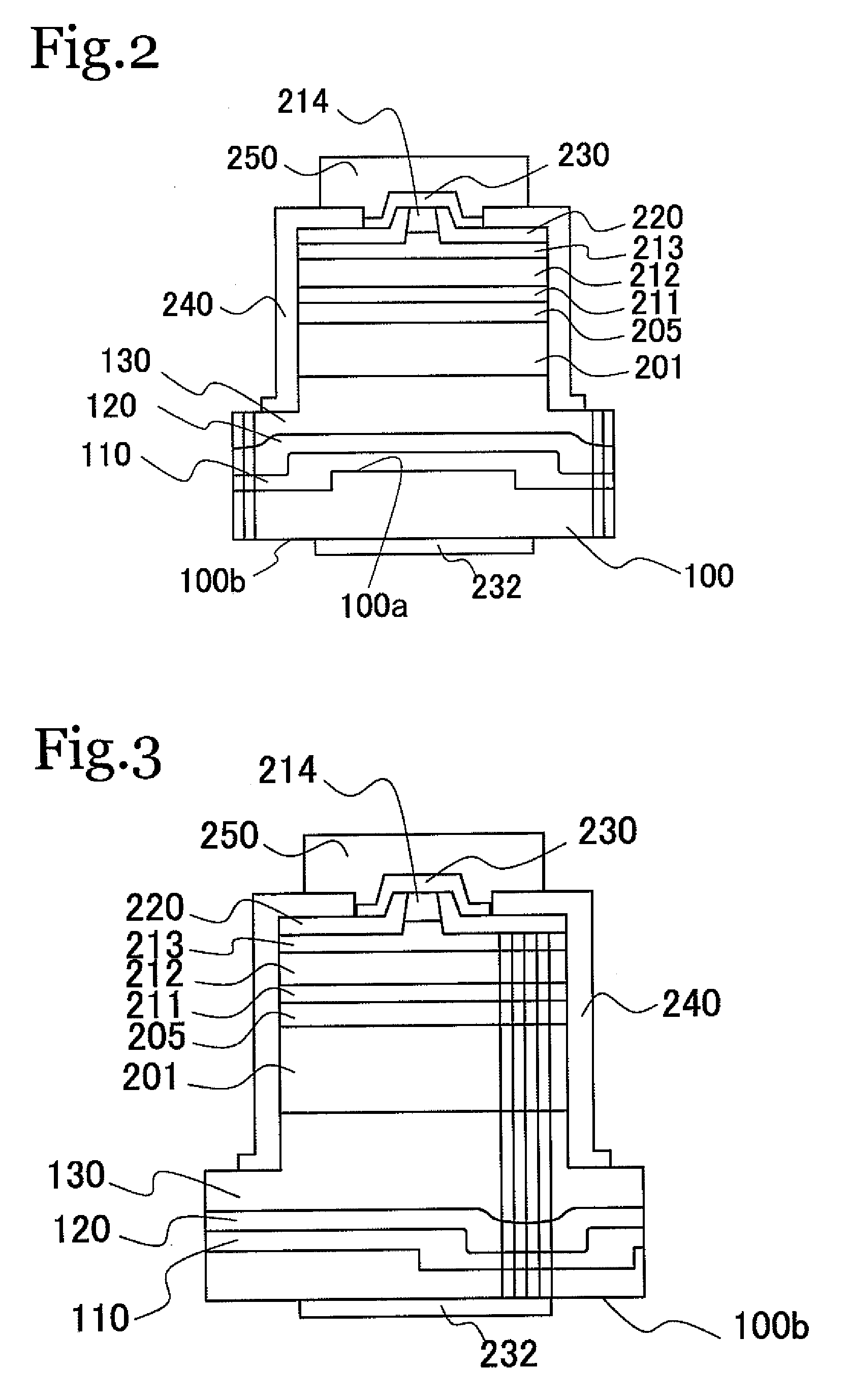
[0044]As shown in FIG. 2, this nitride semiconductor laser element comprises a nitride semiconductor layer laminated on the front side 100a of a nitride semiconductor substrate 100. This nitride semiconductor layer has a first nitride semiconductor layer 110 and a second nitride semiconductor layer 120 in that order from the front side 100a of the nitride semiconductor substrate 100. An active layer 205 and so forth are laminated on this. An-electrode 232 is formed on the rear side 100b of the nitride semiconductor substrate 100.

[0045]Such laser element has a structure wherein the active layer is interposed between a n-type semiconductor layer and a p-type semiconductor layer. The active layer 205 may be a multiple quantum well or single quantum well structure. Also, the laser element of the present invention may be a SCH (Separate Confinement Heterostructure) wherein an optical waveguide is constituted by providing optical guide layers above and below the active layer.

[0046]The man...

embodiment 2

[0118]This nitride semiconductor laser element comprises a nitride semiconductor substrate which has a high dislocation density region and a low dislocation density region containing dislocation density lower than that of the high dislocation density region, and a nitride semiconductor layer laminated thereon, at least one recess is formed at least in the high dislocation density region. The nitride semiconductor layer has a first nitride semiconductor layer in which the grown film thickness in the lateral direction from the side faces of the recess in the substrate is greater than the grown film thickness in the heightwise direction from a region other than the recess. The dislocations extending in the in-plane direction are present in the region of growth of the first nitride semiconductor layer in the lateral direction. Structure and manufacture conditions other than this can be made to be the same as that of the Embodiment 1. Also, a dislocation extending in the in-plane directi...

embodiment 3

[0122]This nitride semiconductor laser element comprises a nitride semiconductor substrate having the dislocation density of no more than 1×10⁷ / cm2 at the substrate surface, and at least one recess is formed in the substrate surface. The nitride semiconductor layer has a first nitride semiconductor layer in which the grown film thickness in the lateral direction from the side faces of the recesses in the substrate is greater than the grown film thickness in the heightwise direction from a region other than the recess. The dislocations extending in the in-plane direction are present in the region of growth of the first nitride semiconductor layer in the lateral direction, the density of these the dislocations extending in the in-plane direction in the region of growth of the first nitride semiconductor layer in the lateral direction is at least 1×10⁸ / cm2. Structure and manufacture conditions other than this can be made to be the same as that of the Embodiments 1 and 2.

[0123]The dislo...


PUM

PropertyMeasurementUnit
sizeaaaaaaaaaa
sizeaaaaaaaaaa
off angleaaaaaaaaaa

Abstract

A nitride semiconductor laser element comprises a nitride semiconductor substrate and a nitride semiconductor layer laminated thereon, wherein the nitride semiconductor substrate has a high dislocation density region and a low dislocation density region containing lower dislocation than that of the high dislocation density region, and has at least one recess formed in at least the high dislocation density region, the nitride semiconductor layer has a first nitride semiconductor layer in which the grown film thickness in the lateral direction from the side faces of the recess in the substrate is greater than the grown film thickness in the heightwise direction from a region other than the recess, and a second nitride semiconductor layer that is disposed on the first nitride semiconductor layer and contains indium, and the first nitride semiconductor layer and second nitride semiconductor layer have recess over the recess in the nitride semiconductor substrate.

Description

BACKGROUND OF THE INVENTION[0001]1. Field of the Invention[0002]The present invention relates to a nitride semiconductor laser element and a method for manufacturing the nitride semiconductor laser element.[0003]2. Background Information[0004]Nitride semiconductor laser elements hold promise as light sources for next-generation optical disks, light sources for displays, and light sources for exposures.[0005]A nitride semiconductor substrate is used for growing a semiconductor layer in a nitride semiconductor laser element. A nitride semiconductor substrate has high dislocation density regions and low dislocation density regions.[0006]A nitride semiconductor layer with a laminar structure is obtained by crystal growth of a nitride semiconductor layer by metal-organic chemical vapor deposition (MOCVD), for example.[0007]Low manufacturing yield is generally a problem with nitride semiconductor laser elements, and the substrate is one of the reasons for this.[0008]At present, a GaN subs...

Claims


Application Information

Patent Timeline
Patent Type & Authority Applications(United States)
IPC IPC(8): H01S5/323H01L33/00B82Y20/00H01S5/343
CPCB82Y20/00H01S5/0202H01S2304/12H01S5/3203H01S5/34333H01S5/22
Inventor MASUI, SHINGOMORIZUMI, TOMONORI
Owner NICHIA CORP
Why Eureka
Try Eureka