Capacitor charging apparatus
Active Publication Date: 2008-03-13
ROHM CO LTD
4 Cites 23 Cited by
AI-Extracted Technical Summary
Problems solved by technology
However, since the correlation between the voltage across the primary coil of a transformer and the output voltage can vary with the turns ratio of the transformer or other conditions, such an arrangement presents a problem of inability to detect the output voltage accurately.
As a result, there may be cases where a drive voltage sufficient to drive the load is not obtained or an overcharging beyond the necessary voltage occurs to consume electric power wastefully.
And such a resistive elements capable of withstanding high voltage must be installed as a chip because it is difficult to incorporate it within an LSI.
This results in a larger number of circuit components and thus a larger packaging area.
Moreover, there may be cases where a diode must be installed backward to prevent the charge stored in the output capacitor from discharging to the ground via the resistive element.
In this case, if the amplitude of the base current is fixed independent of the charging current (i.e., the collector current of the bipolar transistor), then there may be cases where current is spent wastefully or sufficient charging current cannot be obtained.
The collector current of a bipolar transistor is subject to the influence of base current, and if more than necessary amount of base current is supplied for the required charging cu...
View moreBenefits of technology
[0017] 1. An advantage of one embodiment of the present invention is to provide a capacitor charg...
View moreAbstract
A capacitor charging apparatus includes a transformer and an output capacitor charged with current flowing through a secondary coil of the transformer, and charges the output capacitor by performing a switching control of a switching transistor provided on a path leading to a primary coil of the transformer. A switching control unit controls on and off of the switching transistor. A voltage detector monitors a voltage at a tap provided in the secondary coil of the transformer. The switching control unit regards the voltage detected by the voltage detector as an output voltage of the capacitor charging apparatus, and controls the on and off of the switching transistor.
Application Domain
Technology Topic
Image
Examples
- Experimental program(6)
Example
First Embodiment
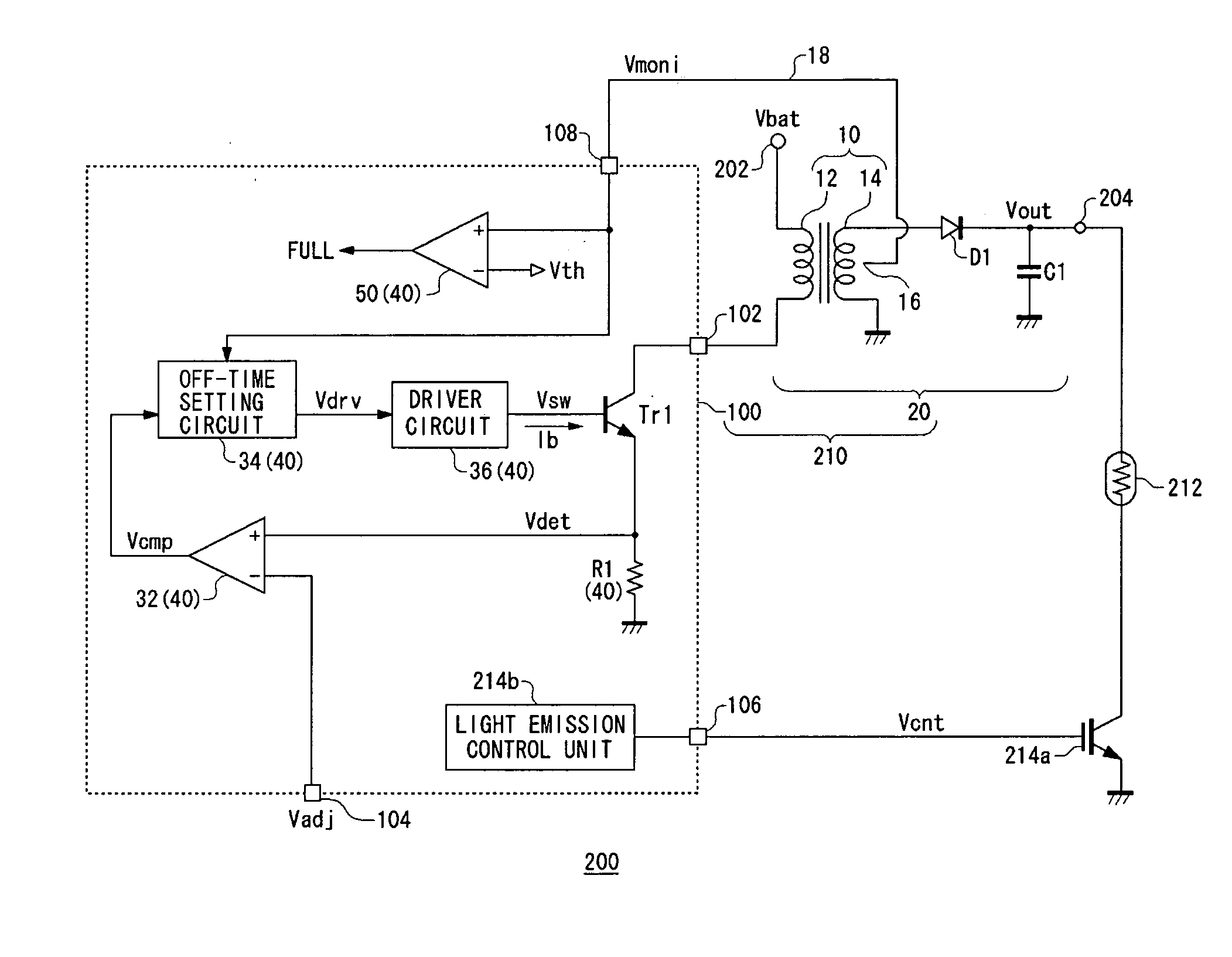
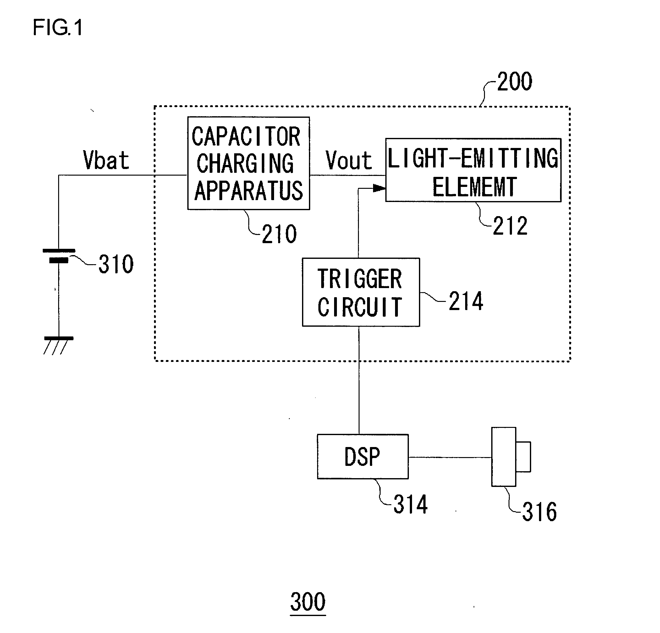
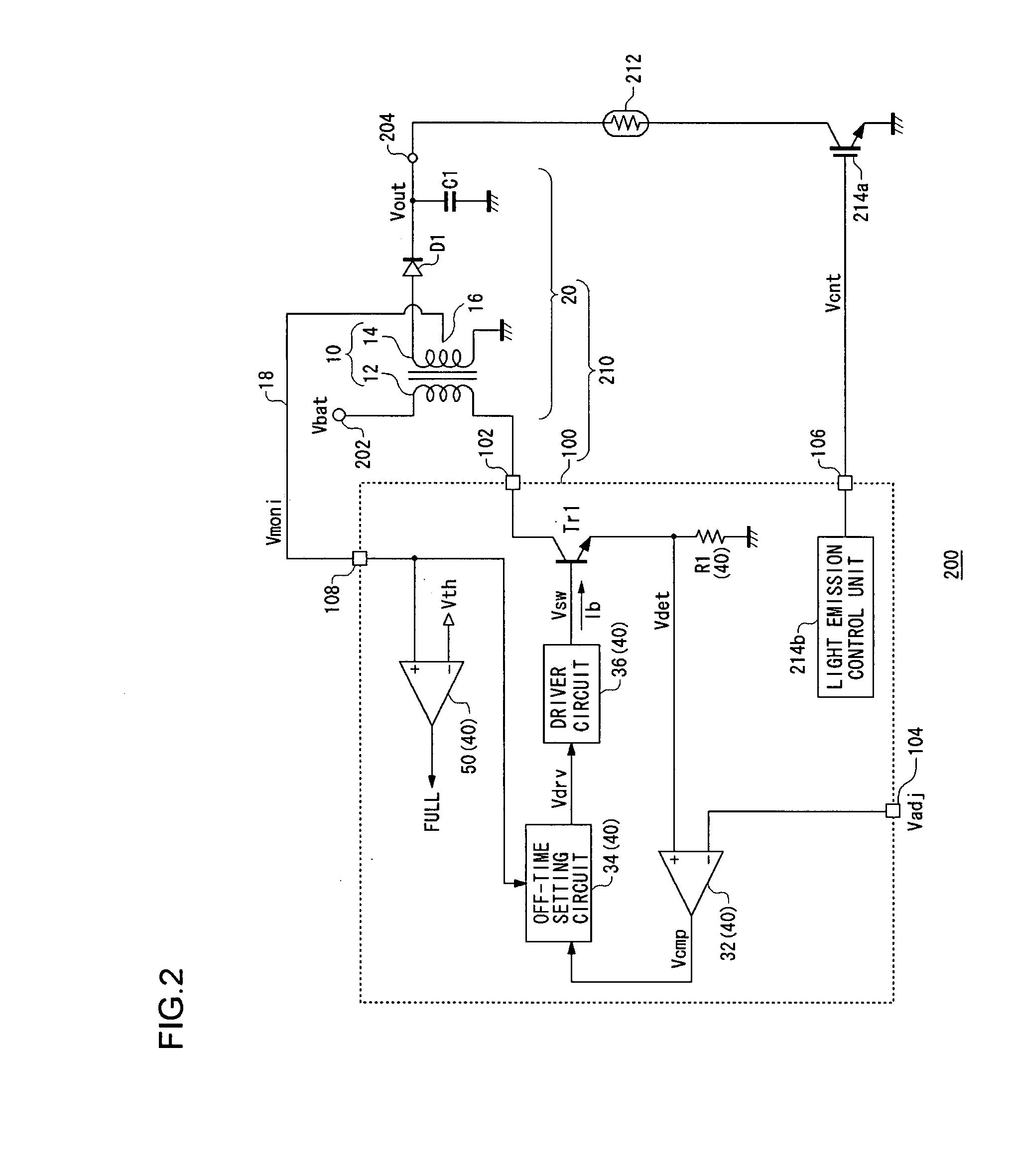
[0094]FIG. 1 is a block diagram showing a structure of an electronic apparatus 300 provided with a light emitting apparatus 200 according to a first embodiment of the present invention. The electronic apparatus 300, which is a digital still camera, a digital video camera or a mobile phone terminal provided with an image pickup function, includes a battery 310, a DSP (Digital Signal Processor) 314, an image pickup unit 316, and a light emitting apparatus 200.
[0095] The battery 310, which is, for instance, a lithium ion battery, outputs a voltage of about 3 to 4 V as a battery voltage Vbat. The DSP 314, which is a block for performing an overall control of the electronic apparatus 300, is connected to the image pickup unit 316 and the light emitting apparatus 200. The image pickup unit 316 is an image-taking device such as a CCD (Charge-Coupled Device) or a CMOS sensor. The light emitting apparatus 200 is a light source that is used as a flash at the time of image pickup by the image pickup unit 316.
[0096] The light emitting apparatus 200 includes a capacitor charging apparatus 210, a light-emitting element 212, and a trigger circuit 214. A xenon tube, for instance, is suitably used as the light-emitting element 212. The capacitor charging apparatus 210 boosts a battery voltage Vbat supplied from the battery 310 by charging an output capacitor provided at the output thereof and supplies a drive voltage of about 300 V to the light-emitting element 212. The trigger circuit 214 is a circuit that controls the light emission timing of the light emitting apparatus 200. The light-emitting element 212 emits light synchronously with the image pickup by the image pickup unit 316.
[0097]FIG. 2 is a circuit diagram showing a structure of a light emitting apparatus 200 of FIG. 1. The light emitting apparatus 200 includes a capacitor charging apparatus 210, a light-emitting element 212 and an IGBT 214a. A control circuit 100, a switching transistor Tr1, a transformer 10, a rectifier diode D1 and an output capacitor C1 shown in FIG. 2 correspond to the capacitor charging apparatus 210 shown in FIG. 1. The trigger circuit 214 shown in FIG. 1 corresponds to the IGBT 214a and the light emission control unit 214b of FIG. 2.
[0098] The capacitor charging apparatus 210 generates a drive voltage (hereinafter referred to also as output voltage Vout) necessary for the light emission by the light-emitting element 212 by supplying a charging current to the output capacitor C1. The capacitor charging apparatus 210 is structured by including an output circuit 20 and a control circuit 100.
[0099] The output circuit 20 includes a transformer 10, a rectifier diode D1, and an output capacitor C1. The transformer 10 is provided with a primary coil 12 and a secondary coil 14. One end of the primary coil 12 is the input terminal 202 of the capacitor charging apparatus 210, where a battery voltage Vbat outputted from the battery 310 of FIG. 1 is applied. The other end of the primary coil 12 is connected to the switching terminal 102 of the control circuit 100.
[0100] One end of the secondary coil 14 of the transformer 10 is grounded to fix the potential, whereas the other end thereof is connected to an anode of the rectifier diode D1. One end of the output capacitor C1 is grounded, and the other end thereof is connected to a cathode of the rectifier diode D1. A terminal of the output capacitor C1 serves as the output terminal 204 of the capacitor charging apparatus 210 and thus outputs the voltage charged in the output capacitor C1 as an output voltage Vout.
[0101] According to the first embodiment, the secondary coil 14 of the transformer 10 is provided with a tap 16 (F winding). The voltage of the tap 16 (hereinafter referred to as monitoring voltage Vmoni) is inputted to a voltage monitoring terminal 108 of the control circuit 100 via a wiring 18. The control circuit 100 controls the on and off of the switching transistor Tr1 by regarding the monitoring voltage Vmoni as the output voltage Vout of the light emitting apparatus 200. The voltage monitoring terminal 108 and the wiring 18 leading to the tap 16 function as a voltage detector that monitors the voltage of the tap 16.
[0102] The control circuit 100 stores energy in the transformer 10, generates a charging current for the output capacitor C1, and boosts the voltage of the battery voltage Vbat by performing a switching control of the on and off of the switching transistor Tr1. Hereinbelow, the current flowing through the primary coil 12 is called a primary current Ic1, and that flowing through the secondary coil 14 a secondary current Ic2.
[0103] The control circuit 100 includes a detection resistor R1, a comparator 32, an off-time setting circuit 34, a driver circuit 36, a light emission control unit 214b, and a charging completion detecting circuit 50, in addition to the switching transistor Tr1. The control circuit 100 is integrated onto a single semiconductor substrate as a function IC.
[0104] The control circuit 100 controls the on and off of the switching transistor Tr1 by controlling the voltage or current that is applied to the control terminal thereof. In this first embodiment, the switching transistor Tr1 is a bipolar transistor. The collector of the switching transistor Tr1 is coupled to the primary coil 12 of the transformer 10 via a switching terminal 102. The driver circuit 36 performs a switching control of the base current Ib of the switching transistor Tr1.
[0105] The detection resistor R1, the comparator 32, the off-time setting circuit 34, the driver circuit 36, and a charging completion detecting circuit 50, in combination, function as a switching control unit for controlling the switching operation of the switching transistor Tr1. This switching control unit controls the on and off of the switching transistor Tr1 by regarding the monitoring voltage Vmoni as the output voltage Vout of the capacitor charging apparatus 210.
[0106] The detection resistor R1 functions as a primary current detection circuit that detects the primary current Ic1 flowing through the primary coil 12 of the transformer 10. The detection resistor R1 is provided on the same path as the primary coil 12 where the primary current Ic1 flows and the switching transistor Tr1 are, and one end thereof is grounded and the other end thereof is connected to the emitter of the switching transistor Tr1. Across the detection resistor R1 occurs a voltage drop (Vdet=Ic1×R1) in proportion to the primary current Ic1. The detection resistor R1 outputs a detection voltage Vdet according to the primary current Ic1.
[0107] To a charging current control terminal 104 of the control circuit 100, a current adjusting signal Vadj, which is used to specify the charging current for the output capacitor C1, is inputted from outside. The comparator 32 compares the detection voltage Vdet outputted from the primary current detection circuit against the current adjusting signal Vadj. The comparator 32 outputs a high-level signal when it detects that the detection voltage Vdet has exceeded the current adjusting signal Vadj, that is, the primary current Ic1 has reached a predetermined current value determined according to the current adjusting signal Vadj (hereinafter referred to as a peak current value Ipeak). A comparison signal Vcmp outputted from the comparator 32 is inputted to the off-time setting circuit 34. As will be described later, the current adjusting signal Vadj is a signal that defines the peak value Ipeak of a charging current. The relationship between the peak current value Ipeak and the current adjusting signal Vadj is expressed as Ipeak=Vadj/R1.
[0108] The off-time setting circuit 34 counts a certain off-time Toff from the point when a comparison signal Vcmp goes high and generates a drive signal Vdrv of a first level (e.g., low level) for a period until this off-time Toff elapses.
[0109] While the drive signal Vdrv is at the first level, i.e., while the off-time Toff is being counted by the off-time setting circuit 34, the driver circuit 36 stops the supply of base current to the switching transistor Tr1, thereby turning off the switching transistor Tr1. As the drive signal Vdrv returns to a second level (e.g., high level) after the lapse of the off-time Toff, the driver circuit 36 supplies base current to the switching transistor Tr1, thereby turning it on again.
[0110] The switching control unit 40 outputs to the base of the switching transistor Tr1 a switching signal Vsw for specifying “on” to the switching transistor Tr1 until the primary current Ic1 reaches a predefined peak current value Ipeak, and then specifying “off” to the switching transistor Tr1 for a period of a certain off-time.
[0111] Note that the off-time Toff may be a predetermined duration of time, may be set according to the output voltage Vout, may be set according to the condition of the primary side or the secondary side of the transformer 10, or may be set according to the monitoring voltage Vmoni as will be explained later.
[0112] Inputted to the driver circuit 36 in the switching control unit 40 is the current adjusting signal Vadj that specifies the charging current. In response to the current adjusting signal Vadj, the driver circuit 36 adjusts the switching signal to be outputted to the base of the switching transistor Tr1. More specifically, the switching control unit 40 adjusts the current value of the base current Ib to be outputted as a switching signal to the base of the switching transistor Tr1, according to the current adjusting signal Vadj.
[0113] The charging completion detecting circuit 50, which is a comparator, detects the completion of a charging by regarding the monitoring voltage Vmoni appearing at the tap 16 provided on the secondary coil 14 of the transformer 10 as the output voltage Vout appearing at the output capacitor C1 and comparing it against a predetermined threshold voltage Vth. The threshold voltage Vth is set to a voltage sufficient for light emission by the light-emitting element 212, for example, about 300 V. Upon detecting the completion of charging, the charging completion detecting circuit 50 sets a flag FULL to indicate the completion of charging. Now with the completion of charging detected by the charging completion detecting circuit 50, the switching control unit 40 stops the switching of the switching transistor Tr1.
[0114] Further, according to the first embodiment, the monitoring voltage Vmoni inputted to the voltage monitoring terminal 108 is inputted to the off-time setting circuit 34 in the switching control unit 40. The off-time setting circuit 34 operates in a manner such that the off-time Toff, during which the switching transistor Tr1 is turned off, changes according to the monitoring voltage Vmoni.
[0115] For example, the off-time setting circuit 34 may set the off-time Toff in such a manner that the higher the monitoring voltage Vmoni is, that is, the higher the output voltage Vout is, the shorter the off-time Toff may be. If the off-time setting circuit 34 is to be structured by a CR time constant circuit capable of charging and discharging the capacitor, then the off-time Toff can be adjusted by changing the charging current or the discharging current according to the monitoring voltage Vmoni.
[0116] The light emission control unit 214b generates a light emission control signal Vcnt and controls the base voltage of the IGBT 214a. When the light emission control signal Vcnt goes to a high level with a charging of the output capacitor C1 completed and sufficient drive voltage Vout generated, the IGBT 214a turns on and the light-emitting element 212 emits light.
[0117] Now a description will be given of an operation of a light emitting apparatus 200 configured as described above. FIG. 3 is a timing chart showing an operation of a capacitor charging apparatus 210 according to the first embodiment. Note that the vertical axis and the horizontal axis of FIG. 3 are enlarged or reduced as appropriate for ease of understanding and also that the waveforms shown are simplified for easier understanding. At time t0, a switching signal Vsw goes to a high level, that is, the switching transistor Tr1 turns on with a base current Ib supplied thereto. With the switching transistor Tr1 turned on, a primary current Ic1 flowing through the primary coil of the transformer 10 increases gradually until time t1 when Vdet>Vadj.
[0118] With Vdet>Vadj, a comparison signal Vcmp, which is outputted from the comparator 32, switches from low level to high level. The off-time setting circuit 34 sets the drive signal Vdrv to a first level (low level) for an off-time Toff after the comparison signal Vcmp has reached a high level. For the duration when the drive signal Vdrv is at a low level, the driver circuit 36 turns off the switching transistor Tr1 by stopping the supply of base current Ib thereto. With the switching transistor Tr1 turned off, the output capacitor C1 is charged with a secondary current Ic2 flowing through the secondary coil 14 of the transformer 10.
[0119] At time t2, after the passage of an off-time Toff from time t1, the drive signal Vdrv switches to a high level. Now, with the drive signal Vdrv at high level, the driver circuit 36 supplies base current Ib to the switching transistor Tr1. By repeating the cycle of operation from time t0 to time t2, the control circuit 100 charges the output capacitor C1 and raises the output voltage Vout.
[0120] If it is so arranged that the off-time Toff to be set by the off-time setting circuit 34 is dependent on the monitoring voltage Vmoni, then the off-time Toff will grow shorter gradually with the rise in the monitoring voltage Vmoni, namely, the rise in the output voltage Vout. Consequently, when the output voltage Vout is low immediately after the start of charging, the energy stored in the transformer is used efficiently, and as the output voltage Vout goes higher, the charging rate can be accelerated. Thus, it is possible to balance the efficiency and the charging rate.
[0121] At time t3, when the monitoring voltage Vmoni reaches the threshold voltage Vth, a flag FULL indicating the completion of a charging is set by the charging completion detecting circuit 50, which enables a light emission by the light-emitting element 212. When the monitoring voltage Vmoni rises to a desired voltage level, the light emission control unit 214b switches the light emission control signal Vcnt to a high level in synchronism with an image pickup by the image pickup unit 316 as shown in FIG. 1. As a result, the IGBT 214a turns on, and the xenon lamp, which is the light-emitting element 212, emits light as a flash.
[0122] With the capacitor charging apparatus 210 according to the first embodiment, it is possible to detect with accuracy the voltage relative to the output voltage Vout appearing at the output capacitor C1 by monitoring the potential at a tap (F winding) provided on the secondary coil 14 of the transformer 10. Also, location of the tap 16 on the grounding side, namely the lower-voltage side, of the secondary coil 14 makes it unnecessary to use resistance voltage division, thus avoiding any increase in the number of circuit components used. The control circuit 100 can optimally perform switching control of the switching transistor Tr1 using the monitoring voltage Vmoni corresponding to the output voltage Vout.
[0123] For example, according to the first embodiment, the charging completion detecting circuit 50 carries out the detection of a charging state based on the monitoring voltage Vmoni. Compared with the direct monitoring of the output voltage Vout appearing at the output capacitor C1, this arrangement makes it possible to stop the switching by detecting a full charging state with high accuracy. This will also solve the problems of inability to obtain the voltage required to drive the load or overcharging of the output capacitor C1.
[0124] Also, according to the first embodiment, the off-time setting circuit 34 sets the off-time Toff based on the monitoring voltage Vmoni. As a result, the output voltage can be reflected in the switching operation with accuracy.
[0125] The above embodiment is merely exemplary and it is understood by those skilled in the art that various modifications to the combination of each component and process thereof are possible and such modifications are also within the scope of the present invention.
[0126] In the present embodiment, a description has been given of a case where a bipolar transistor is used as the switching transistor Tr1. However, a MOSFET may be used instead. Also, in the present embodiment, a description has been given of a case where the timing of on and off of the switching transistor Tr1 is determined based on the primary current Ic1. However, the control method is not limited thereto, and other control methods may be employed.
[0127] Further, in the present embodiment, a description has been given of a case where a capacitor charging apparatus 210 drives a light-emitting element 212. However, the application is not limited thereto, and the capacitor charging apparatus 210 may also be used to drive a variety of other load circuits that require high voltage.
[0128] Also, the setting of logical values of high level and low level described in the present embodiment is only one example. The setting can be changed freely by inverting them as appropriate by an inverter or the like.
Example
Second Embodiment
[0129]FIG. 4 is a circuit diagram showing a structure of a light emitting apparatus 200a according to a second embodiment of the present invention. Similar to the light emitting apparatus 200 according to the first embodiment, the light emitting apparatus 200a as shown in FIG. 4 is suitably used for the electronic apparatus as shown FIG. 1.
[0130] The electronic apparatus 300 of FIG. 1, which is a digital still camera, a digital video camera or a mobile phone terminal provided with an image pickup function, includes a battery 310, a DSP (Digital Signal Processor) 314, an image pickup unit 316, and a light emitting apparatus 200a.
[0131] The battery 310, which is, for instance, a lithium ion battery, outputs a voltage of about 3 to 4 V as a battery voltage Vbat. The DSP 314, which is a block for performing an overall control of the electronic apparatus 300, is connected to the image pickup unit 316 and the light emitting apparatus 200a. The image pickup unit 316 is an image-taking device such as a CCD (Charge-Coupled Device) or a CMOS sensor. The light emitting apparatus 200a is a light source that is used as a flash at the time of image pickup by the image pickup unit 316.
[0132] The light emitting apparatus 200a includes a capacitor charging apparatus 210, a light-emitting element 212, and a trigger circuit 214. A xenon tube or the like is suitably used as the light-emitting element 212. The capacitor charging apparatus 210 boosts a battery voltage Vbat supplied from the battery 310 by charging an output capacitor provided at the output thereof and supplies a drive voltage of about 300 V to the light-emitting element 212. The trigger circuit 214 is a circuit that controls the light emission timing of the light emitting apparatus 200a. The light-emitting element 212 emits light synchronously with the image pickup by the image pickup unit 316.
[0133] Referring back to FIG. 4, a structure of the light emitting apparatus 200a will now be described. The light emitting apparatus 200a includes a capacitor charging apparatus 210, a light-emitting element 212, and an IGBT 214a. A control circuit 100, a switching transistor Tr1, a transformer 10, a rectifier diode D1 and an output capacitor C1 shown in FIG. 4 correspond to the capacitor charging apparatus 210 shown in FIG. 1. The trigger circuit 214 shown in FIG. 1 corresponds to the IGBT 214a and the light emission control unit 214b of FIG. 4.
[0134] The capacitor charging apparatus 210 generates a drive voltage (hereinafter referred to also as output voltage Vout) necessary for the light emission by the light-emitting element 212 by supplying a charging current to the output capacitor C1. The capacitor charging apparatus 210 is structured by including an output circuit 20 and a control circuit 100.
[0135] The output circuit 20 includes a transformer 10, a rectifier diode D1, and an output capacitor C1. The transformer 10 is provided with a primary coil 12 and a secondary coil 14. One end of the primary coil 12 is the input terminal 202 of the capacitor charging apparatus 210, where the battery voltage Vbat outputted from the battery 310 of FIG. 1 is applied. The other end of the primary coil 12 is connected to the switching terminal 102 of the control circuit 100.
[0136] One end of the secondary coil 14 of the transformer 10 is grounded to fix the potential, whereas the other end thereof is connected to an anode of the rectifier diode D1. One end of the output capacitor C1 is grounded, and the other end thereof is connected to a cathode of the rectifier diode D1. A terminal of the output capacitor C1 serves as the output terminal 204 of the capacitor charging apparatus 210 and thus outputs the voltage charged in the output capacitor C1 as an output voltage Vout.
[0137] The control circuit 100 stores energy in the transformer 10, generates a charging current for the output capacitor C1, and boosts the voltage of the battery voltage Vbat by performing a switching control of the on and off of the switching transistor Tr1. Hereinbelow, the current flowing through the primary coil 12 is called a primary current Ic1, and that flowing through the secondary coil 14 a secondary current Ic2.
[0138] The control circuit 100 includes a detection resistor R1, a comparator 32, an off-time setting circuit 34, a driver circuit 36 and a light emission control unit 214b, in addition to the switching transistor Tr1. The control circuit 100 is integrated onto a single semiconductor substrate as a function IC.
[0139] The control circuit 100 controls the on and off of the switching transistor Tr1 by controlling the voltage or current that is applied to the control terminal thereof. In this second embodiment, the switching transistor Tr1 is a bipolar transistor. The collector of the switching transistor Tr1 is coupled to the primary coil 12 of the transformer 10 via the switching terminal 102. The driver circuit 36 performs a switching control of the base current Ib of the switching transistor Tr1.
[0140] The detection resistor R1 functions as a primary current detection circuit 30 that detects the primary current Ic1 flowing through the primary coil 12 of the transformer 10. The detection resistor R1 is provided on the same path as the primary coil 12 where the primary current Ic1 flows and the switching transistor Tr1 are, and one end thereof is grounded and the other end thereof is connected to the emitter of the switching transistor Tr1. Across the detection resistor R1 occurs a voltage drop (Vdet=Ic1×R1) in proportion to the primary current Ic1. The detection resistor R1 outputs a detection voltage Vdet according to the primary current Ic1.
[0141] To a charging current control terminal 104 of the control circuit 100, a current adjusting signal Vadj, which is used to specify the charging current for the output capacitor C1, is inputted from outside. The comparator 32 compares the detection voltage Vdet outputted from the primary current detection circuit 30 against the current adjusting signal Vadj. The comparator 32 outputs a high-level signal when it detects that the detection voltage Vdet has exceeded the current adjusting signal Vadj, that is, the primary current Ic1 has reached a predetermined peak current value determined according to the current adjusting signal Vadj (hereinafter referred to as a peak current value Ipeak). A comparison signal Vcmp outputted from the comparator 32 is inputted to the off-time setting circuit 34. As will be described later, the current adjusting signal Vadj is a signal that defines the peak value Ipeak of a charging current. The relationship between the peak current value Ipeak and the current adjusting signal Vadj is expressed as Ipeak=Vadj/R1.
[0142] The off-time setting circuit 34 generates a derive signal Vdrv of a first level (e.g., low level) for a period when a comparison signal Vcmp goes high until a certain off-time Toff elapses. While the drive signal Vdrv is in the first level, the driver circuit 36 stops the supply of base current to the switching transistor Tr1 and thereby turns off the switching transistor Tr1. As the drive signal Vdrv returns to a second level (e.g., high level) after the lapse of the off-time Toff, the driver circuit 36 supplies base current to the switching transistor Tr1 and turns it on again.
[0143] That is, according to the second embodiment, the comparator 32, the off-time setting circuit 34 and the driver circuit 36 monitor at least the primary current Ic1 detected by the primary current detection circuit 30 and function as a switching control unit 40 that controls the on and off of the switching transistor Tr1. This switching control unit 40 outputs to the base of the switching transistor Tr1 a switching signal Vsw specifying “on” to the switching transistor for a period until the primary current Ic1 has reached a predetermined peak current value Ipeak and then specifying “off” to the switching transistor Tr1 for a period of a certain off-time.
[0144] Note that the off-time Toff may be a predetermined duration of time, may be set according to the output voltage Vout, or may be set according to the condition of the primary side or the secondary side of the transformer 10.
[0145] Inputted to the driver circuit 36 in the switching control unit 40 is the current adjusting signal Vadj that specifies the charging current. In response to the current adjusting signal Vadj, the driver circuit 36 adjusts the switching signal to be outputted to the base of the switching transistor Tr1. More specifically, the switching control unit 40 adjusts the current value of the base current Ib to be outputted as a switching signal to the base of the switching transistor Tr1, according to the current adjusting signal Vadj.
[0146]FIG. 5 is a circuit diagram showing a structure of the driver circuit 36 of FIG. 4. The driver circuit 36 includes a current generation unit 38. The current generation unit 38 includes, for example, a VI conversion circuit 38a and a current amplifier circuit 38b. The VI conversion circuit 38a receives a current adjusting signal Vadj and generates a current Idrv1 according to the voltage value of the current adjusting signal Vadj. The VI conversion circuit 38a generates the drive current Idrv in such a manner that the larger the current adjusting signal Vadj is, the larger the drive current Idrv1 is. Preferably, the drive current Idrv1 may be proportional to the current adjusting signal Vadj.
[0147] The current Idrv1 is amplified by the current amplifier circuit 38b configured by a current mirror circuit and the like. For a period when the drive signal Vdrv outputted from the off-time setting circuit 34 is in a second level, the switch circuit 39 outputs the drive current Idrv2 as the drive current Ib of the switching transistor Tr1, whereas for a period when the derive signal Vdrv is in a first level, it stops the output of the drive current Idrv2.
[0148] Refer back to FIG. 4. The charging completion detecting circuit 50 monitors either directly or indirectly the output voltage Vout appearing at the output capacitor C1. “Directly monitoring” includes a case where the potential of the output terminal 204 is subjected to the resistance voltage division. “Indirectly monitoring” includes a case where the voltage applied to the primary coil 12 or the secondary coil 14 of the transformer 10 is monitored.
[0149] The charging completion detecting circuit 50, which is a comparator, detects the completion of a charging by comparing an output voltage Vout′ corresponding to the output voltage Vout against a predetermined threshold voltage Vth. The threshold voltage Vth is set to a voltage sufficient for light emission by the light-emitting element 212, for example, about 300 V. Upon detecting the completion of charging, the charging completion detecting circuit 50 sets a flag FULL to indicate the completion of charging. Now with the completion of charging detected by the charging completion detecting circuit 50, the switching control unit 40 stops the switching of the switching transistor Tr1.
[0150] The light emission control unit 214b generates a light emission control signal Vcnt and controls the base voltage of the IGBT 214a. When the light emission control signal Vcnt goes to a high level with a charging of the output capacitor C1 completed and sufficient drive voltage Vout generated, the IGBT 214a turns on and the light-emitting element 212 emits light.
[0151] Now a description will be given of an operation of a light emitting apparatus 200a configured as described above. FIG. 6 is a timing chart showing an operation of a capacitor charging apparatus 210 according to the second embodiment. Note that the vertical axis and the horizontal axis of FIG. 6 are enlarged or reduced as appropriate for ease of understanding and also that the waveforms shown are simplified for easier understanding.
[0152] At time t0, a switching signal Vsw goes to a high level, that is, the switching transistor Tr1 turns on with a base current Ib supplied thereto. With the switching transistor Tr1 turned on, a primary current Ic1 flowing through the primary coil of the transformer 10 increases gradually until time t1 when Vdet>Vadj.
[0153] With Vdet>Vadj, a comparison signal Vcmp, which is outputted from the comparator 32, switches from low level to high level. The off-time setting circuit 34 sets the drive signal Vdrv to a first level (low level) for an off-time Toff after the comparison signal Vcmp has become a high level. For the duration when the drive signal Vdrv is at a low level, the driver circuit 36 turns off the switching transistor Tr1 by stopping the supply of base current Ib thereto. With the switching transistor Tr1 turned off, the output capacitor C1 is charged with a secondary current Ic2 flowing through the secondary coil 14 of the transformer 10.
[0154] At time t2, after the passage of an off-time Toff from time t1, the drive signal Vdrv switches to a high level. Now, with the drive signal Vdrv at high level, the driver circuit 36 supplies base current Ib to the switching transistor Tr1. By repeating the cycle of operation from time t0 to time t2, the control circuit 100 charges the output capacitor C1 and raises the output voltage Vout.
[0155] At time t3, when the output voltage Vout reaches the threshold voltage Vth, a flag FULL indicating the completion of a charging is set, thereby enabling a light emission by the light-emitting element 212. When the output voltage Vout rises to a desired voltage level, the light emission control unit 214b switches the light emission control signal Vcnt to a high level in synchronism with an image pickup by the image pickup unit 316 as shown in FIG. 1. As a result, the IGBT 214a turns on, and the xenon lamp, which is the light-emitting element 212, emits light as a flash.
[0156]FIGS. 7A to 7C are timing charts each showing a base current Ib supplied to a switching transistor Tr1 and a primary current Ic1. FIG. 7A illustrates a case where the current adjusting signal Vadj is small and therefore the charging current is set to a small value, whereas FIG. 7C illustrates a case where the current adjusting signal Vadj is set to a maximum value and therefore the charging current is also maximum. FIG. 7B illustrates an intermediate case of the charging current in between the above two cases. The driver circuit 36 sets the level of the base current Ib in accordance with the current adjusting signal Vadj, namely the peak value Ipeak of the primary current Ic1. As a result, the base current Ib in the case of FIG. 7B is larger than that in the case of FIG. 7A.
[0157] In the capacitor charging apparatus 210 according to the second embodiment, the charging current is set in response to the peak current Ipeak of the primary current Ic1. It is required that the base current in response to a collector current (i.e., primary current Ic1) be supplied in order to stably drive a bipolar transistor. Thus, in a case when the level of the base current Ib is to be fixed to a constant value, it is required that a base current associated with the maximum value Imax of an assumed peak current Ipeak be set beforehand. In FIGS. 7A to 7C, such a base current is shown as a dotted line. In this case, when a charging current lower than the maximum value Imax is set, a base current larger than the normally required base current is supplied to the switching transistor Tr1 and therefore a wasteful power will be consumed.
[0158] In contrast to this, the capacitor charging apparatus 210 according to the second embodiment adjusts the base current Ib in response to the charging current, namely, the primary current Ic1 flowing through the switching transistor Tr1 as a collector current. Accordingly, in a case when the primary current Ic1 is small, the base current Ib is also set to a small value, thus preventing the wasteful consumption of current.
[0159] The above-described embodiments are merely exemplary, and it is understood by those skilled in the art that various modifications to the combination of each component and process thereof are possible and such modifications are also within the scope of the present invention.
[0160] In the above embodiments a description has been given of a case where a bipolar transistor is used as the switching transistor Tr1, but a MOSFET may be used instead. In such a case, too, the same suitable drive as in the case of the bipolar can be realized. That is, if the level of charging current is large, a gate drive current may be increased or the amplitude of gate voltage may be set to a large value.
[0161] In the above embodiments a description was given of a case where the capacitor charging apparatus 210 drives the light emitting element 212, but this should not be considered as liming, and it can drive a variety of other load circuits requiring high voltage.
[0162] In the above embodiments, the setting of logical values of high level and low level is one example among many and it may be arbitrarily changed as appropriate by inversion by an inverter or the like.
Example
Third Embodiment
[0163]FIG. 1 is a block diagram showing a structure of an electronic apparatus 300 outfitted with a light emitting apparatus 200c according to a third embodiment of the present invention. An electronic apparatus 300, which is a digital still camera, a digital video camera or a mobile phone terminal provided with an image pickup function, includes a battery 310, a DSP (Digital Signal Processor) 314, an image pickup unit 316, and a light emitting apparatus 200c.
[0164] The battery 310, which is, for instance, a lithium ion battery, outputs a voltage of about 3 to 4 V as a battery voltage Vbat. The DSP 314, which is a block for performing an overall control of the electronic apparatus 300, is connected to the image pickup unit 316 and the light emitting apparatus 200c. The image pickup unit 316 is an image-taking device such as a CCD (Charge-Coupled Device) or a CMOS sensor. The light emitting apparatus 200c is a light source that is used as a flash at the time of image pickup by the image pickup unit 316.
[0165] The light emitting apparatus 200c includes a capacitor charging apparatus 210, a light-emitting element 212, and a trigger circuit 214. A xenon tube or the like is suitably used as the light-emitting element 212. The capacitor charging apparatus 210 boosts a battery voltage Vbat supplied from the battery 310 by charging an output capacitor provided at the output thereof and supplies a drive voltage of about 300 V to the light-emitting element 212. The trigger circuit 214 is a circuit that controls the light emission timing of the light emitting apparatus 200c. The light-emitting element 212 emits light synchronously with the image pickup by the image pickup unit 316.
[0166]FIG. 8 is a circuit diagram showing a structure of the light emitting apparatus 200c according to the third embodiment. The light emitting apparatus 200c includes a capacitor charging apparatus 210, a light-emitting element 212, and an IGBT 214a. A control circuit 100c, a switching transistor Tr1, a transformer 10, a rectifier diode D1 and an output capacitor C1 shown in FIG. 8 correspond to the capacitor charging apparatus 210 shown in FIG. 1. The trigger circuit 214 shown in FIG. 1 corresponds to the IGBT 214a and the light emission control unit 214b of FIG. 8.
[0167] The capacitor charging apparatus 210 generates a drive voltage (hereinafter referred to also as output voltage Vout) necessary for the light emission by the light-emitting element 212 by supplying a charging current to the output capacitor C1. The capacitor charging apparatus 210 is structured by including an output circuit 20 and a control circuit 100c.
[0168] The output circuit 20 includes a transformer 10, a rectifier diode D1, and an output capacitor C1. The transformer 10 is provided with a primary coil 12 and a secondary coil 14. One end of the primary coil 12 is the input terminal 202 of the capacitor charging apparatus 210, where the battery voltage Vbat outputted from the battery 310 of FIG. 1 is applied. The other end of the primary coil 12 is connected to the switching terminal 102 of the control circuit 100c.
[0169] One end of the secondary coil 14 of the transformer 10 is grounded to fix the potential, whereas the other end thereof is connected to an anode of the rectifier diode D1. One end of the output capacitor C1 is grounded, and the other end thereof is connected to a cathode of the rectifier diode D1. A terminal of the output capacitor C1 serves as an output terminal 204 of the capacitor charging apparatus 210 and thus outputs the voltage charged in the output capacitor C1 as an output voltage Vout.
[0170] The control circuit 100c stores energy in the transformer 10, generates a charging current for the output capacitor C1, and boosts the voltage of the battery voltage Vbat by performing a switching control of the on and off of the switching transistor Tr1. Hereinbelow, the current flowing through the primary coil 12 is called a primary current Ic1, and that flowing through the secondary coil 14 a secondary current Ic2.
[0171] The control circuit 100c includes an off-signal generator 80, a first on-signal generator 90, a second on-signal generator 96, a switching control unit 60 and a charging completion detecting circuit 70, in addition to the switching transistor Tr1. The control circuit 100c is integrated onto a single semiconductor substrate as a function IC.
[0172] The off-signal generator 80 monitors the primary current Ic1 flowing through the primary coil 12 of the transformer 10, and outputs an off signal Soff when the primary current Ic1 increases up to and reaches a predetermined peak current Ipeak. The off-signal generator 80 includes a first resistor R1 and a first comparator 82. The detection resistor R1 is provided on the same path as the primary coil 12 where the primary current Ic1 flows and the switching transistor Tr1 are, and one end thereof is grounded and the other end thereof is connected to the emitter of the switching transistor Tr1. Across the detection resistor R1 occurs a voltage drop (Vdet=Ic1×R1) in proportion to the primary current Ic1. The detection resistor R1 outputs a detection voltage Vdet according to the primary current Ic1.
[0173] To a charging current control terminal 104 of the control circuit 100c, a current adjusting signal Vadj, which is used to specify the charging current for the output capacitor C1, is inputted from outside. The first comparator 82 compares the detection voltage Vdet outputted from the primary current detection circuit against the current adjusting signal Vadj. The first comparator 82 outputs a high-level off signal Soff when it detects that the detection voltage Vdet has exceeded the current adjusting signal Vadj, that is, the primary current Ic1 has reached a predetermined current value determined according to the current adjusting signal Vadj (hereinafter referred to as peak current value Ipeak). The off signal Soff outputted from the first comparator 82 is inputted to the switching control unit 60 and the second on-signal generator 96. The relationship between the peak current value Ipeak and the current adjusting signal Vadj is expressed as Ipeak=Vadj/R1.
[0174] The switching terminal 102 of the control circuit 100c is connected to one end of the primary coil 12. The battery voltage Vbat outputted from the battery 310 is inputted to an input voltage terminal 110. A second comparator 94 shifts a voltage appearing at the switching terminal 102 to the high-potential side by a first threshold voltage Vth1 generated from a voltage supply 92 so as to compare it with the battery voltage Vbat inputted to the input terminal 110. If ΔV 1, a high-level signal (hereinafter referred to as first on signal Son1) will be outputted from the second comparator 94. That is, the first on-signal generator 90 monitors the voltage ΔV across the primary coil 12 of the transformer 10; and if the voltage ΔV across the primary coil 12 drops down to the first threshold voltage Vth1, the first on-signal generator 90 will output a high-level first on signal Son1. The first on signal Son1 is inputted to the switching control unit 60.
[0175] The monitoring voltage Vout′ corresponding to the output voltage Vout appearing at the output capacitor C1 is inputted to a voltage monitoring terminal 108 of the control circuit 100c. The monitoring voltage Vout′ is a voltage obtained when the output voltage Vout is voltage-divided by a resistor R2 and a resistor R3. The monitoring voltage Vout′ is inputted to the second on-signal generator 96.
[0176] The second on-signal generator 96 monitors the monitoring voltage Vout′ and then sets an off-time Toff based on this monitoring voltage Vout′. When the off signal Soff of high level is outputted from the off-signal generator 80 and then the off-time thus set has elapsed, the second on-signal generator 96 outputs the second on signal Son2 of high level.
[0177] For example, the second on-signal generator 96 sets the off-time Toff in a manner that the larger the monitoring voltage Vout′ is, namely, the larger the output voltage Vout is, the shorter the off-time Toff will become. For example, the second on-signal generator 96 can be structured by a CR time-constant circuit which charges/discharges a capacitor. In such a case, the off-time Toff can be suitably adjusted by varying the charging or discharging current according to the monitoring voltage Vout′. Also, the second on-signal generator 96 may be constituted by a digital timer.
[0178] The switching control unit 60 receives the off signal Soff outputted from the off-signal generator 80, and the first on signal Son1 and the second on signal Son2 outputted from the first on-signal generator 90 and the second on-signal generator 96, respectively. The switching control unit 60 turns off the switching transistor Tr1 in response to the off signal Soff and turns on the switching transistor Tr1 in response to the first on signal Son1 and the second on signal Son2.
[0179] In the third embodiment, the switching control unit 60 includes a flip-flop 62 and a driver circuit 64. By a switch SW1, either one of the first on signal Son1 and the second on signal Son2 is outputted to the flip-flop 62. The switch SW1 may be controlled by a user. The off signal Soff is inputted to a reset terminal of the flip-flop 62. That is, when a high level is inputted to a set terminal of the flip-flop 62 by either the first on signal Son1 or the second on signal Son2, an output signal Sq of the flip-flop 62 goes to a high level. When a high level is inputted to the reset terminal of the flip-flop 62, the output signal Sq goes to a low level.
[0180] The driver circuit 64 outputs a switching signal Vsw in response to the output signal Sq of the flip-flop 62, to the base of the switching transistor Tr1. The driver circuit 64 turns on the switching transistor Tr1 when the output signal Sq of the flip-flop 62 is in a high level, whereas the driver circuit 64 turns off the switching transistor Tr1 when the output signal Sq thereof is in a low level.
[0181] The charging completion detecting circuit 70, which is a comparator, detects the completion of a charging by comparing a monitoring voltage Vout′ against a predetermined threshold voltage Vth3. The threshold voltage Vth3 is set to a voltage sufficient for light emission by the light-emitting element 212, for example, about 300 V. When the monitoring voltage Vout′ exceeds the threshold voltage Vth3, the charging completion detecting circuit 70 sets a flag FULL to indicate the completion of charging. Now with the completion of charging detected by the charging completion detecting circuit 70, the switching control unit 60 stops the switching of the switching transistor Tr1.
[0182] The light emission control unit 214b generates a light emission control signal Vcnt and controls the base voltage of the IGBT 214a. When the light emission control signal Vcnt goes to a high level with a charging of the output capacitor C1 completed and sufficient drive voltage Vout generated, the IGBT 214a turns on and the light-emitting element 212 emits light.
[0183] Now a description will be given of an operation of the light emitting apparatus 200c configured as described above. FIGS. 9 and 10 are each a timing chart showing an operation of a capacitor charging apparatus 210 according to the third embodiment. FIG. 9 shows a switching operation in response to the first on signal Son1, whereas FIG. 10 shows a switching operation in response to the second on signal Son2. Note that the vertical axis and the horizontal axis of FIG. 9 and FIG. 10 are enlarged or reduced as appropriate for ease of understanding and also that the waveforms shown therein are simplified for easier understanding.
[0184] With reference to FIG. 9, a description is first given of a charging operation according to the off signal Soff and the first on signal Son1. At time t0, a switching signal Vsw goes to a high level and therefore the switching transistor Tr1 turns on. At this time, the output signal Sq of the flip-flop is in a high level.
[0185] With the switching transistor Tr1 turned on, a primary current Ic1 flowing through the primary coil 12 of the transformer 10 gradually increases with time and this increase in the primary current Ic1 causes the detection voltage Vdet to rise.
[0186] When Vdet>Vadj at time t1, namely when the primary current Ic1 has reached the peak current value Ipeak, the off signal Soff outputted from the first comparator 82 goes to a high level. Then the flip-flop 62 is reset and, as a result, the output signal Sq transits to a low level. As the output signal Sq goes to the low level, the switching signal Vsw goes also to a low level, thereby turning off the switching transistor Tr1.
[0187] For a period of time t0 to t1 during which the switching transistor Tr1 is on, the voltage across the primary coil 12 is ΔV≈Vbat−Vsat. Here, Vsat is the sum voltage of an emitter-collector voltage of the switching transistor Tr1 and the detection voltage Vdet.
[0188] As the switching transistor Tr1 turns off at time t1, the energy stored in the transformer 10 is discharged as a secondary current Ic2. The secondary current Ic2 flows into the output capacitor C1 as a charging current and the output voltage Vout rises. When the energy stored in the transformer 10 has been completely expended at time t2, the output voltage Vout stops rising.
[0189] During a period of time t1 to t2, the voltage ΔV across the primary coil 12 is ΔV≈Vout/n. Here, n is a turns ratio of the primary coil 12 and the secondary coil 14 of the transformer 10. When the energy stored in the transformer 10 has been completely discharged at time t2, the voltage ΔV across the primary coil 12 damped-oscillates due to the LC oscillation. As the voltage ΔV across the primary coil 12 becomes less than the first threshold voltage Vth1 at time t3, the second comparator 94 outputs the first on signal Son1 of high level. This first on signal Son1 sets the flip-flop 62, so that the output signal Sq transits to a high level and the switching transistor Tr1 turns on again.
[0190] By repeating the cycle of operation from t1 to t3, the control circuit 100c charges the output capacitor C1. This charging operation raises the output voltage Vout. And when the monitoring voltage Vout′ has reached the threshold voltage Vth3 at time t4, a flag FULL indicating the completion of charging is set by the charging completion detecting circuit 70, which enables a light emission by the light-emitting element 212. After the charging has been completed, the light emission control unit 214b switches the light emission control signal Vcnt to a high level in synchronism with an image pickup by the image pickup unit 316 as shown in FIG. 1. As a result, the IGBT 214a turns on, and the xenon lamp, which is the light-emitting element 212, emits light as a flash.
[0191] Next, with reference to FIG. 10, a description is given of a charging operation according to the off signal Soff and the second on signal Son2. At time t0, the output signal Sq of the flip-flop 62 goes to a high level, thereby turning on the switching transistor Tr1.
[0192] With the switching transistor Tr1 turned on, the primary current Ic1 flowing through the primary coil 12 of the transformer 10 gradually increases with time, which in turn raises the detection voltage Vdet.
[0193] With Vdet>Vadj at time t1, the off signal Soff outputted from the first comparator 82 goes to a high level, the flip-flop 62 is reset and the output signal Sq thereof transits to a low level. As the output signal Sq goes to the low level, the switching signal Vsw also goes to a low level, thus turning off the switching transistor Tr1.
[0194] As the switching transistor Tr1 turns off at time t1, the energy stored in the transformer 10 is discharged as a secondary current Ic2. The secondary current Ic2 flows into the output capacitor C1 as a charging current and the output voltage Vout rises.
[0195] The second on-signal generator 96 outputs a second on signal Son2 which goes to a high level from time t1 when a high-level off signal Soff is outputted until time t2 after the passage of an off-time Toff set according to the monitoring voltage Vout′. The flip-flop 62 is set by this second on signal Son2, then the output signal Sq shifts to a high level and the switching transistor Tr1 turns on again.
[0196] By repeating the cycle of operation from t0 to t2, the control circuit 100c charges the output capacitor C1 and raises the output voltage Vout. When the monitoring voltage Vout′ has reached the threshold voltage Vth3 at time t3, a flag FULL indicating the completion of charging is set by the charging completion detecting circuit 70, which enables a light emission by the light-emitting element 212.
[0197] In the control performed based on the first on signal Son1 of the capacitor charging apparatus 210 according to the third embodiment, the switching transistor Tr1 is turned on after the energy stored in the transformer 10 has been completely discharged. Hence, the high efficiency can be realized. Also, by performing the control based on the second on signal Son2, the energy can be used efficiently, immediately after a start of charging, because of a longer off-time. Hence, as the output voltage Vout increases, the charge rate can be accelerate with a shorter off-time.
[0198] Further, by employing the capacitor charging apparatus 210 according to the third embodiment, the control can be switched between the control based on the first on signal Son1 as shown in FIG. 9 and the control based on the second on signal Son2 as shown in FIG. 10. As a result, either a circuit operation where the efficiency is given priority or a circuit operation where the charge rate is given priority can be selected according to its application or the like.
Login to view more PUM


Description & Claims & Application Information
We can also present the details of the Description, Claims and Application information to help users get a comprehensive understanding of the technical details of the patent, such as background art, summary of invention, brief description of drawings, description of embodiments, and other original content. On the other hand, users can also determine the specific scope of protection of the technology through the list of claims; as well as understand the changes in the life cycle of the technology with the presentation of the patent timeline. Login to view more.
Login to view more Similar technology patents
Frequency control circuit suitable for fixed off time control mode boost converter
InactiveCN101951149ASimple circuit structureReliable functionDc-dc conversionElectric variable regulationAsic technologyIntegrated circuit
Owner:FUDAN UNIV
Over-temperature protection circuit
ActiveCN104967095ASimple circuit structureLow number of componentsEmergency protective arrangements for automatic disconnectionPower managementHysteresis
Owner:UNIV OF ELECTRONIC SCI & TECH OF CHINA
New energy automobile charging gun with charging gun head achieving temperature protection function
ActiveCN105655815ASimple circuit structureNo additional controllerVehicle connectorsCharging stationsGround lineEngineering
Owner:绵阳高新区探索科技有限责任公司
Shift register unit, driving method, gate drive circuit and display device
ActiveCN108288451ASimple circuit structureReduces component count and space occupied by signal linesStatic indicating devicesDigital storageEngineeringClock signal
Owner:BOE TECH GRP CO LTD +1
Shift register unit and gate drive device
ActiveCN102708777ASimple circuit structureLess signal wiringStatic indicating devicesClock signalShift register
Owner:BOE TECH GRP CO LTD +1
Classification and recommendation of technical efficacy words
- Simple circuit structure
Backlight source driving circuit and driving circuit thereof as well as liquid crystal television
ActiveCN102243850ASimple and easy circuit implementationSimple circuit structureTelevision system detailsStatic indicating devicesMultiple componentLiquid crystal
Owner:HISENSE VISUAL TECH CO LTD
Electric-heating full-automatic soybean milk machine with fuzzy control
ActiveCN102160575AGreat tasteSimple circuit structureBeverage vesselsMilk substitutesRise rateElectric heating
Owner:KINGCLEAN ELECTRIC
Interleaved parallel PFC control circuit and control method
ActiveCN101594049ASolve the uneven flow problemSimple circuit structureEfficient power electronics conversionPower conversion systemsCarrier signalWave shape
Owner:EMERSON NETWORK POWER CO LTD
Contactless method of supplying power
InactiveUS20130285618A1Simple circuit structureLow manufacturing costBatteries circuit arrangementsElectromagnetic wave systemForeign objectPower output
Owner:DEPUY PROD INC +1
Direct-current power flow controller for multiport flexible direct-current power transmission system and control method
InactiveCN104184139ASimple circuit structureFewer switching devicesDc network circuit arrangementsElectric power transfer ac networkInductorPower flow
Owner:SOUTHEAST UNIV