Photomask having self-masking layer and methods of etching same

a self-masking layer and photomask technology, applied in the field of photomasks, can solve the problems of affecting performance, affecting the etch rate, and the technological limit of present optical lithography techniques, and achieve the effect of low etch ra

Active Publication Date: 2008-03-20
APPLIED MATERIALS INC
View PDF9 Cites 7 Cited by
  • Summary
  • Abstract
  • Description
  • Claims
  • Application Information

AI Technical Summary

Problems solved by technology

Thus, any defects in the mask may be transferred to the chip, potentially adversely affecting performance.
Defects that are severe enough may render the mask completely useless.
However, with the shrinking of critical dimensions of the mask (corresponding to the shrinking dimensions of the transistors and electrical circuits formed in the ICs), present optical lithography techniques are approaching their technological limit.
This etch bias issue mainly results from erosion of photoresist.
During pattern transfer, the photoresist is consumed significantly because of the limited etch rate selectivity of the absorber layer to the photoresist.
This consumption of photoresist lowers the fidelity of the pattern transfer process.

Method used


Image

  • Photomask having self-masking layer and methods of etching same
  • Photomask having self-masking layer and methods of etching same
  • Photomask having self-masking layer and methods of etching same

Examples


Embodiment Construction

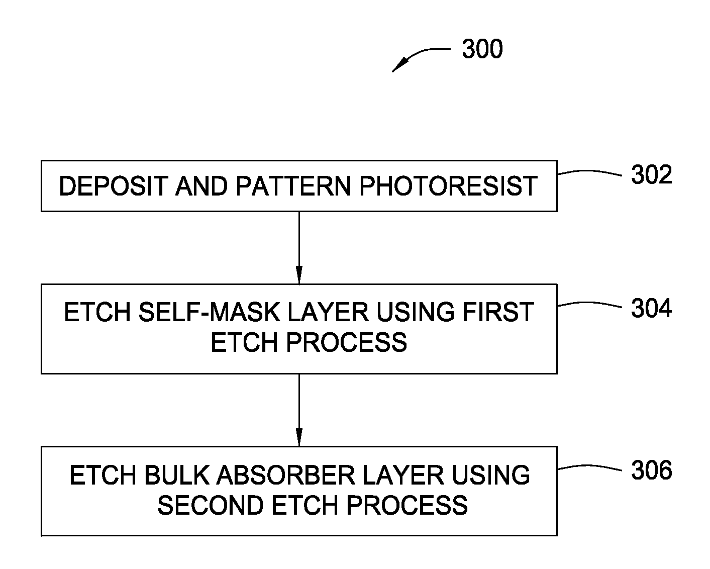
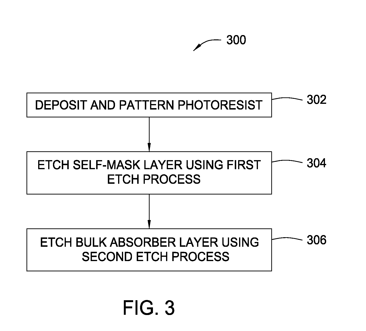
[0017]The present invention provides a photomask structure and method of etching that can be used for optical binary photomask, embedded attenuated phase shift mask (EAPSM), and alternate aperture phase shift mask (AAPSM) applications to reduce the etch CD bias and improve pattern transfer fidelity as compared to conventional masks.

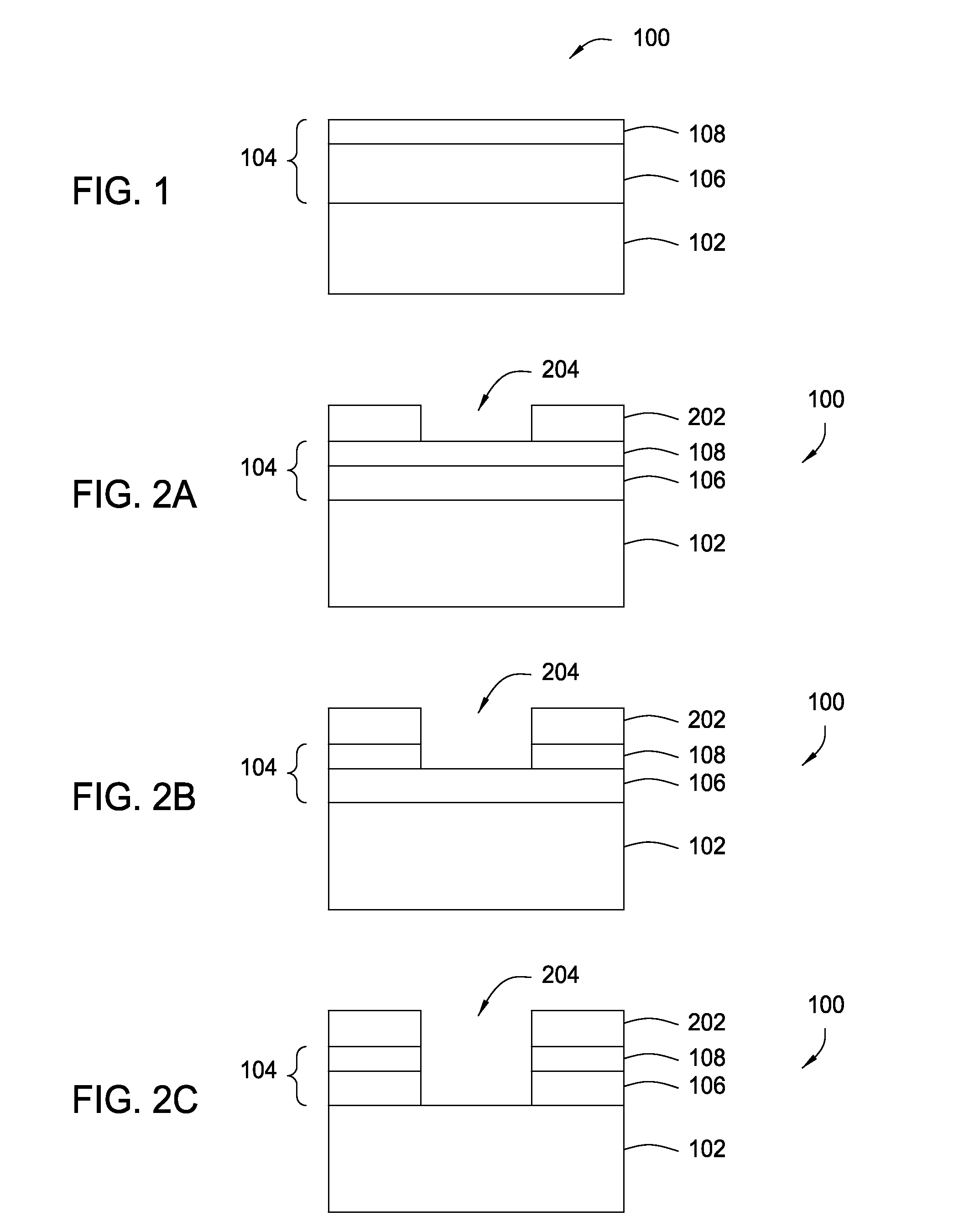
[0018]FIG. 1 depicts one embodiment of a blank photomask, or mask, 100 of the present invention. As depicted in FIG. 1, the mask 100 includes an optically transparent substrate 102 having a multi-layer absorber layer 104. The substrate 102 may typically comprise an optically transparent silicon based material, such as quartz (e.g., silicon dioxide, SiO2), and the like. The substrate 102 may be any size suitable for use as a photomask. In one embodiment, the substrate 102 has a rectangular shape having sides between about 5-9 inches in length. The substrate 102 may be about 0.15-0.25 inches thick. In one embodiment, the substrate 102 is about 0.25 inches t...


PUM

PropertyMeasurementUnit
thicknessaaaaaaaaaa
lengthaaaaaaaaaa
thickaaaaaaaaaa

Abstract

A photomask structure and method of etching is provided herein. In one embodiment, a photomask includes a translucent substrate and an opaque multi-layer absorber layer disposed over the substrate. The opaque multi-layer absorber layer comprises a self-mask layer disposed over a bulk absorber layer. The self-mask layer comprises one of nitrogenized tantalum and silicon-based materials (TaSiON), tantalum boron oxide-based materials (TaBO), or oxidized and nitrogenized tantalum-based materials (TaON). The bulk absorber layer comprises on of tantalum silicide-based materials (TaSi), nitrogenized tantalum boride-based materials (TaBN), or tantalum nitride-based materials (TaN). The self-mask layer has a low etch rate during the bulk absorber layer etch step, thereby acting as a hard mask.

Description

BACKGROUND OF THE INVENTION[0001]1. Field of the Invention[0002]Embodiments of the present invention generally relate photomasks used in the fabrication of semiconductor devices, more specifically, to a photomask having a self-masking layer and methods of etching thereof.[0003]2. Description of the Related Art[0004]In the manufacture of integrated circuits (IC), or chips, patterns representing different layers of the chip are created by a chip designer. A series of reusable photomasks (also referred to herein as masks) are created from these patterns in order to transfer the design of each chip layer onto a semiconductor substrate during the manufacturing process. Mask pattern generation systems use precision lasers or electron beams to image the design of each layer of the chip onto a respective mask. The masks are then used much like photographic negatives to transfer the circuit patterns for each layer onto a semiconductor substrate. These layers are built up using a sequence of ...

Claims


Application Information

Patent Timeline
Patent Type & Authority Applications(United States)
IPC IPC(8): B32B17/10B32B9/00B32B17/06G03F1/00
CPCG03F1/14G03F1/80G03F1/58G03F1/30Y10T428/31616
Inventor WU, BANQIU
Owner APPLIED MATERIALS INC
Why Eureka
Try Eureka