Electroluminescent Display Apparatus and Methods

a technology of electroluminescent display and display apparatus, which is applied in the direction of discharge tube luminescnet display, discharge tube/lamp details, electric discharge lamps, etc., can solve the problems of not all materials offering sufficient chemical stability and compatibility in the presence of high processing temperature and/or high electric fields, and achieves flexible, scalable, and high-performance el display. , the effect of easy manufacturing

Inactive Publication Date: 2008-03-27
NANOLUMENS ACQUISITION
View PDF0 Cites 3 Cited by
  • Summary
  • Abstract
  • Description
  • Claims
  • Application Information

AI Technical Summary

Benefits of technology

[0023]Embodiments of this invention thus provide a high performance EL display that is flexible, scalable, and easily manufactured. The present invention also provides efficient and cost effective methods for manufacturing a flexible EL display that allows testing of EL performance prior to final assembly, thereby facilitating improved quality control and decreasing manufacturing costs.

Problems solved by technology

Below this critical voltage, the phosphor layer may experience electric fields, but the electric field is not sufficient to generate light in the phosphor layer, and so the EL device is in its dark or off state.
These dielectrics do not exhibit the properties required to work well in layers adjacent to oxide phosphors, which have high threshold electric fields.
While all of these dielectrics exhibit a sufficiently high figure of merit (defined as the product of the breakdown electric field and the relative dielectric constant) to function in the presence of high electric fields, not all of these materials offer sufficient chemical stability and compatibility in the presence of high processing temperatures and / or high electric fields.
But at temperatures significantly higher than 500° C., glass softens and mechanical deformation occurs due to stresses within the glass.
Because some phosphors require processing temperatures greater than 500° C., the use of a glass substrate limits the types of phosphors that can be used in the typical TFEL manufacturing process.
Although these dielectrics offer good breakdown protection due to their thickness, they limit the processing temperature that can be applied to phosphors that are on top of the dielectric layer.
Phosphors that require processing temperatures of 700° C. or higher may be contaminated by diffusion from the dielectric formulation of the thick film dielectrics.
Also, substrate cost is much higher for ceramics than for glass, particularly for large size ceramics over 30 cm in length or width, since cracking and warping of large ceramic sheets is hard to control.
In addition to high temperature mechanical deformation, a further disadvantage of using glass and similar substrates is the rigidity of the resulting display.
But the design and manufacturing techniques of many displays, such as LCD and plasma displays do not lend themselves to scalability of larger displays due to weight, cost, and efficiency issues.
An additional problem with present displays and manufacturing methods is in the area of quality control.
Under current methods it is difficult to test whether the display will properly “light up” until a substantial portion of the manufacturing process is completed which leads to costly quality control techniques and high repair and replacement costs.
For example, if a display is tested only after completion and a defect is found, then the repair of the display is more costly, and even if the display is repaired, it will typically be sold on a secondary market at decreased margins.
Furthermore, the phosphors used in prior art displays are moisture-sensitive and are therefore not open-atmosphere-tolerant, thus requiring that the phosphors be protected under glass.
Not only does this make the display rigid as discussed above, but the manufacture of some types of displays, such as LCD displays, requires expensive manufacturing techniques, such as clean-room processing techniques.

Method used


Image

  • Electroluminescent Display Apparatus and Methods
  • Electroluminescent Display Apparatus and Methods
  • Electroluminescent Display Apparatus and Methods

Examples


Embodiment Construction

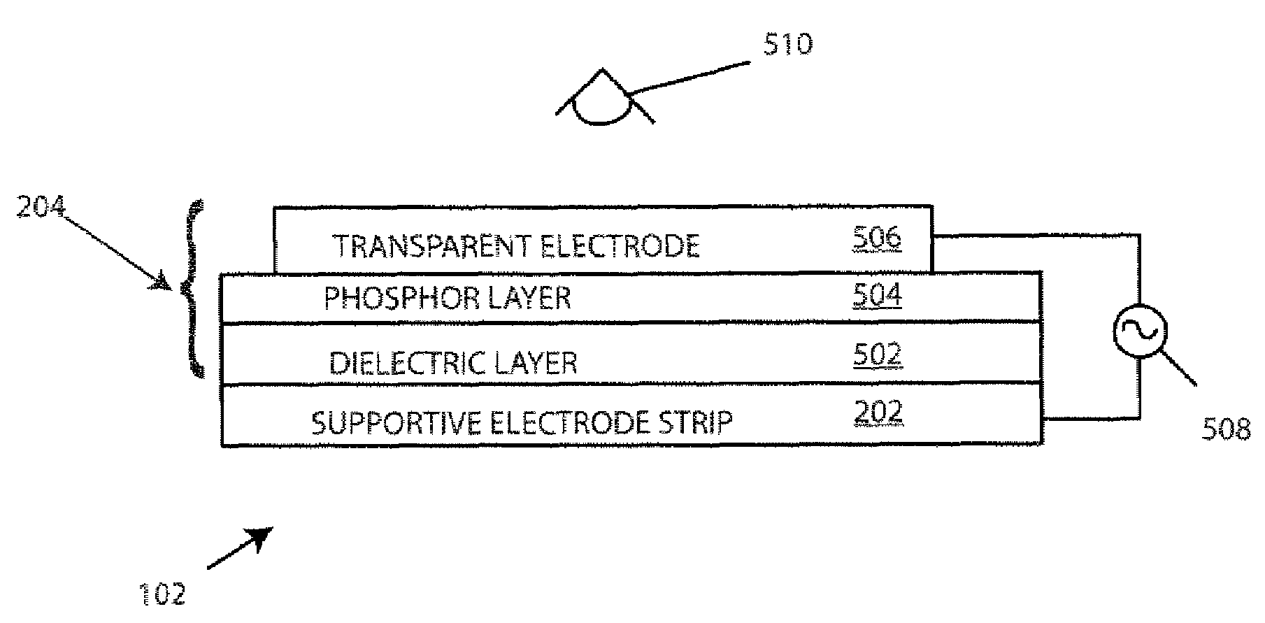
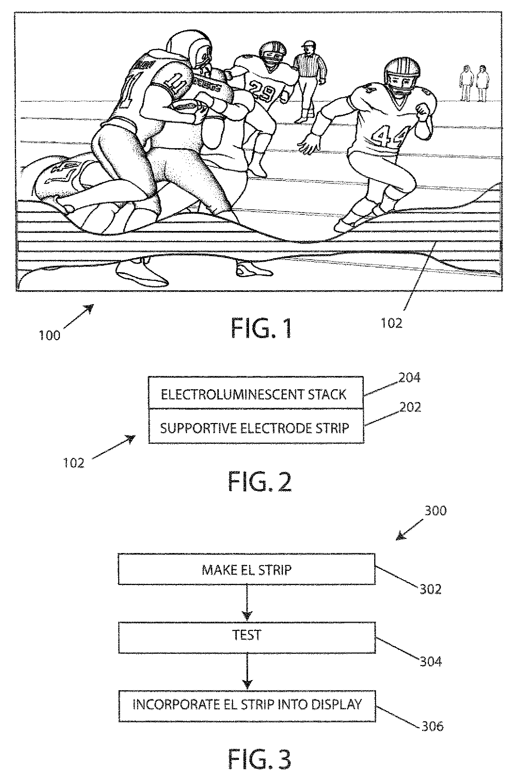
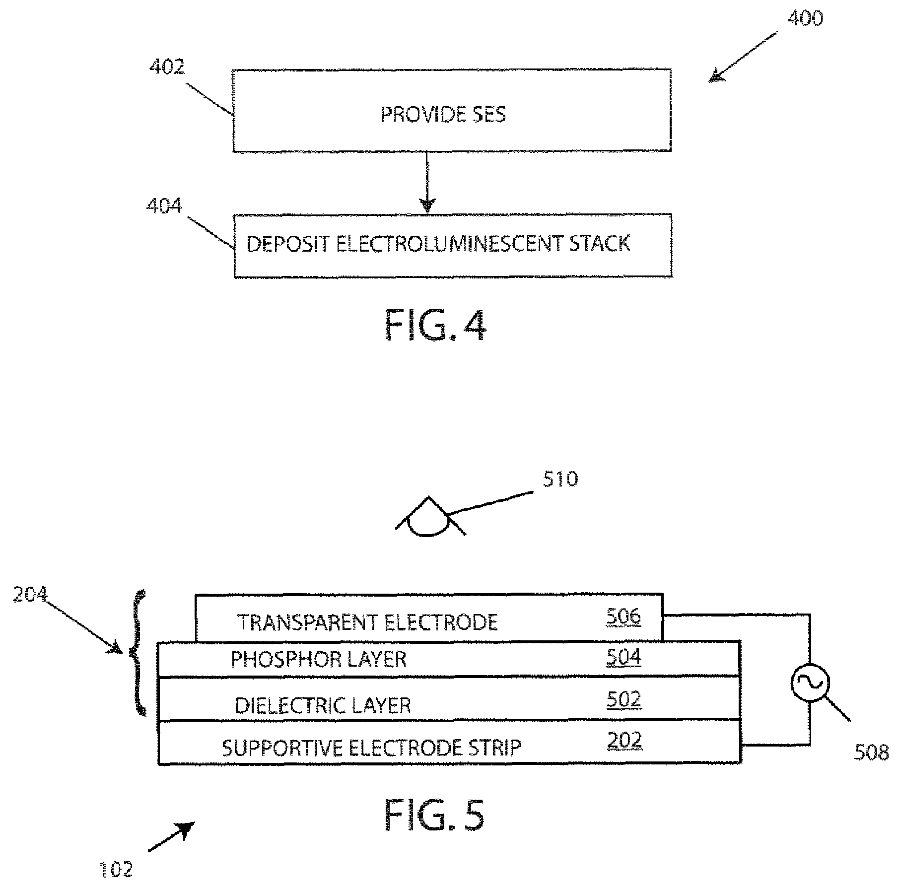
[0046]Generally speaking, the systems, methods, and apparatus taught herein are directed to an EL apparatus and an improved electroluminescent (EL) display incorporating the EL apparatus. By applying what is taught herein a flexible, rugged, and sealable EL display can be made.

[0047]As required, exemplary embodiments of the present invention are disclosed. These embodiments are meant to be examples of various ways of implementing the invention and it will be understood that the invention may be embodied in alternative forms. The figures are not to scale and some features may be exaggerated or minimized to show details of particular elements, while related elements may have been eliminated to prevent obscuring novel aspects. Therefore, specific structural and functional details disclosed herein are not to be interpreted as limiting, but merely as a basis for the claims and as a representative basis for teaching one skilled in the art to variously employ the present invention.

[0048]In...


PUM


Abstract

The present invention provides apparatus, methods and systems for an electroluminescent (EL) display. An exemplary embodiment of an EL apparatus of the invention is in the form of an EL strip. The EL strip may comprise a Supportive Electrode Strip (SES) adapted to receive an EL stack, and an EL stack deposited thereon. The SES comprises a conductive substrate. The EL stack deposited on the SES to form an EL strip may include several layers. The EL strips may be grouped together to form an EL strip panel. The EL strips may also be electrically connected to form an EL panel and EL panels can be electrically connected to form an EL display. Methods for making and testing such systems and components are also disclosed.

Description

FIELD OF THE INVENTION[0001]The present invention relates to electroluminescent displays, and more particularly to methods and systems for manufacturing electroluminescent apparatus and flexible electroluminescent displays.BACKGROUND OF THE INVENTION[0002]Display devices are available that employ the phenomenon of Electroluminescence (EL), which is the conversion of electrical energy to light by a solid phosphor subjected to an electric field. A type of EL device known as a Thin Film Electroluminescent (TFEL) device has shown the desirable qualities of long life, wide operating temperature range, high contrast, wide viewing angle and high brightness.[0003]TFEL devices typically include a laminate or laminar stack of thin films deposited on a substrate; wherein the laminate comprises an EL phosphor material and an insulating layer sandwiched between a pair of electrode layers. EL laminates are substrate-based devices that are typically manufactured in a “front to rear” method beginni...

Claims


Application Information

Patent Timeline
Patent Type & Authority Applications(United States)
IPC IPC(8): H01J1/62H01J63/04
CPCH05B33/26
Inventor KITAI, ADRIAN H.SUMMERS, CHRISTOPHER J.WAGNER, BRENT K.COPE, RICHARD C.
Owner NANOLUMENS ACQUISITION
Why Eureka
Try Eureka