Method of manufacturing complementary metal oxide semiconductor transistor

a technology of complementary metal oxide and semiconductor transistor, which is applied in the direction of semiconductor devices, electrical equipment, basic electric elements, etc., can solve the problems of component efficacy loss and excessive depletion of silicon substrates of source/drain

Active Publication Date: 2008-04-10
UNITED MICROELECTRONICS CORP
View PDF32 Cites 70 Cited by
  • Summary
  • Abstract
  • Description
  • Claims
  • Application Information

AI Technical Summary

Benefits of technology

[0017]The present invention does not need to deposit a cap layer on the substrate, and therefore does not influence the continuous recess etching process as in the prior art. The present invention forms a patterned block layer utilizing the dielectric layer, which forms the spacer. The spacer etching process forms the patterned block layer, and the process of removing the spacer can remove the block layer. Therefore, the manufacture of the present invention is simpler than the prior art.

Problems solved by technology

When a salicide (self-aligned silicide) process is performed on a small transistor, the silicon substrates of the source / drain are depleted excessively.
This results in the crystal lattices of the source / drain being damaged, and the PN junction between the source / drain and the substrate being too close to the silicide, causing leakage, and the component to lose efficacy.

Method used


Image

  • Method of manufacturing complementary metal oxide semiconductor transistor
  • Method of manufacturing complementary metal oxide semiconductor transistor
  • Method of manufacturing complementary metal oxide semiconductor transistor

Examples


Embodiment Construction

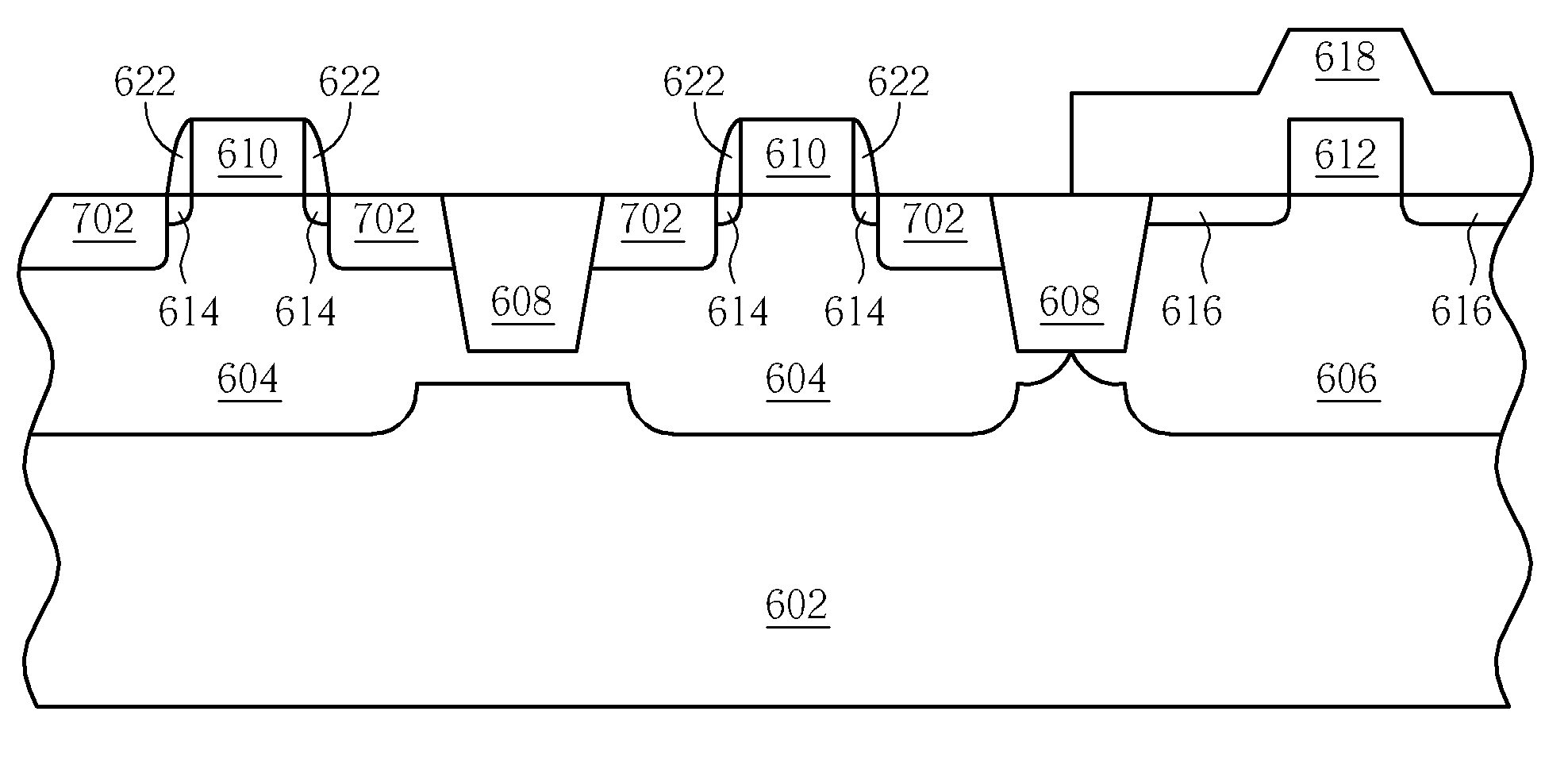
[0022]The present invention relates to a method of forming a PMOS transistor, an NMOS transistor, and a CMOS transistor. It applies to strained-silicon MOS transistors or a selective epitaxial growth (SEG) process that builds the source / drain of the transistor high.

[0023]Please refer to FIGS. 6 to 11. FIGS. 6 to 11 are schematic diagrams of manufacturing a CMOS transistor according to the first embodiment of the present invention. As FIG. 6 shows, a substrate 602 could be a P type silicon substrate, an N type silicon substrate, or a silicon on insulation (SOI) in the first embodiment. The substrate 602 includes an N well 604, a P well 606, and a shallow trench isolation (STI) 608. A plurality of gate structures 610 and 612 are deposited on the substrate 602. The gate structure 610 is formed on the N well 104; the gate structure 612 is formed on the P well 606, and the STI 608 is formed between the adjacent gate structures 610 and 612 in the substrate 602. The gate structures 610, 61...


PUM


Abstract

A method of manufacturing a CMOS is disclosed. A substrate has a first gate and a second gate. A dielectric layer and a patterned photo-resist layer are formed sequentially on the substrate. After an etching process, the dielectric layer without the photo-resist layer forms a spacer around the first gate, and the dielectric layer with the photo-resist layer forms a block layer on the second gate. The recesses are formed in the substrate of two lateral sides of the first gate. The epitaxial silicon layers are formed in the recesses.

Description

BACKGROUND OF THE INVENTION[0001]1. Field of the Invention[0002]The present invention relates to a method of manufacturing a complementary metal oxide semiconductor transistor (CMOS). The feature of the present invention is that there is no additional process for forming the cap layer as the hard mask of the continued recess etching process and the selective epitaxial growth.[0003]2. Description of the Prior Art[0004]As semiconductor components become smaller, transistor manufacture has been improved significantly in order to manufacture transistors of small volume and high quality. When a salicide (self-aligned silicide) process is performed on a small transistor, the silicon substrates of the source / drain are depleted excessively. This results in the crystal lattices of the source / drain being damaged, and the PN junction between the source / drain and the substrate being too close to the silicide, causing leakage, and the component to lose efficacy.[0005]Therefore, current transisto...

Claims


Application Information

Patent Timeline
Patent Type & Authority Applications(United States)
IPC IPC(8): H01L21/8238
CPCH01L21/823807H01L21/823814H01L29/7848H01L29/66628H01L29/66636H01L29/165
Inventor SHIH, HUNG-LINCHU, TSAN-CHI
Owner UNITED MICROELECTRONICS CORP
Why Eureka
Try Eureka