Emr sensor and transistor formed on the same substrate

a technology of emr sensor and transistor, applied in the field of magnetic sensing system, can solve the problem that the emr sensor b>100/b> described above is difficult to fabricate, and achieve the effect of cost-effective fabrication

Inactive Publication Date: 2008-04-17
WESTERN DIGITAL TECH INC
View PDF15 Cites 19 Cited by
  • Summary
  • Abstract
  • Description
  • Claims
  • Application Information

AI Technical Summary

Benefits of technology

[0007]The invention solves the above and other related problems by fabricating an EMR sensor and transistor(s) connected in a signal amplifying circuit on the same magnetic sensing chip. The EMR sensor and the transistor(s) may comprise substantially similar or identical heterostructures. For instance, the transistor(s) may be a high electron mobility transistor (HEMT) where a subset of the multilayer structure forms a quantum well comprising a two-dimensional electron gas (2DEG) or hole gas (2DHG). Similarly, the EMR sensor is a multilayer structure where a subset of the multilayer structure forms a quantum well comprising a 2DEG or 2DHG. Thus, the EMR sensor and the transistor(s) may be formed on a common substrate with the same layers in the same deposition steps. Magnetic sensing chips can be fabricated more cost effectively by forming both the EMR sensor and the transistor(s) in the same fabrication steps.
[0008]Further, the EMR sensor and the transistor(s) may advantageously be fabricated closer together on the same magnetic sensing chip, which produces a compact design. The close proximity of the EMR sensor and the transistor(s) can also reduce the capacitance between the conductors that connect the EMR sensor to the transistor(s) leading to reduced noise and faster response.

Problems solved by technology

The EMR sensor 100 described above is difficult to fabricate.

Method used


Image

  • Emr sensor and transistor formed on the same substrate
  • Emr sensor and transistor formed on the same substrate
  • Emr sensor and transistor formed on the same substrate

Examples


Embodiment Construction

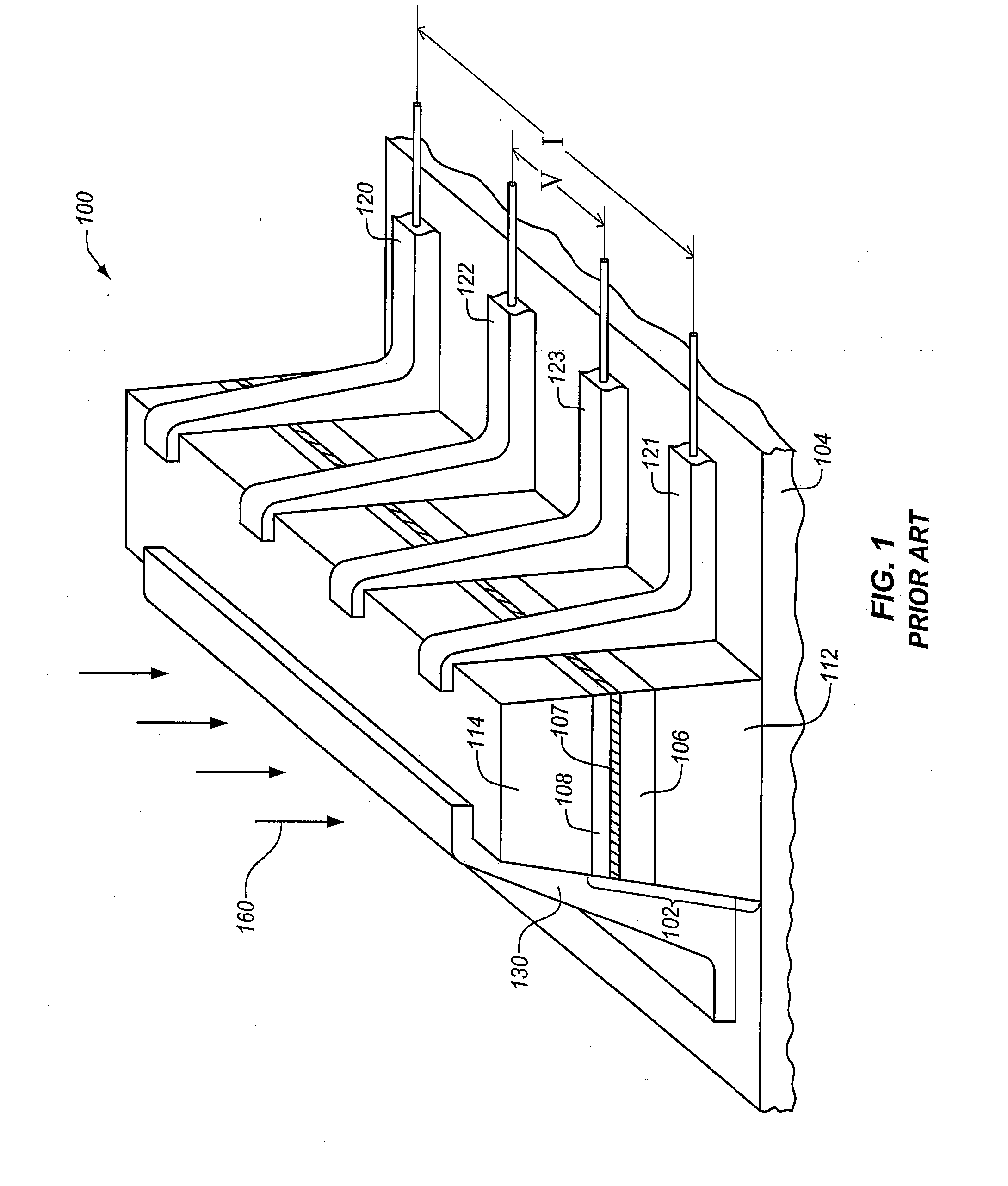
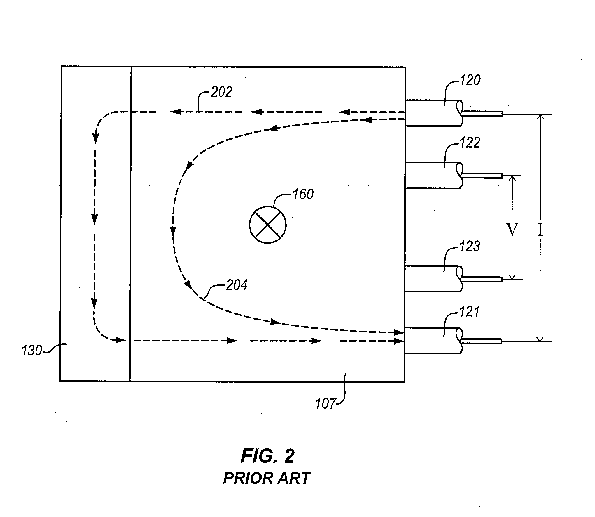
Description of Prior Art—FIGS. 1-2

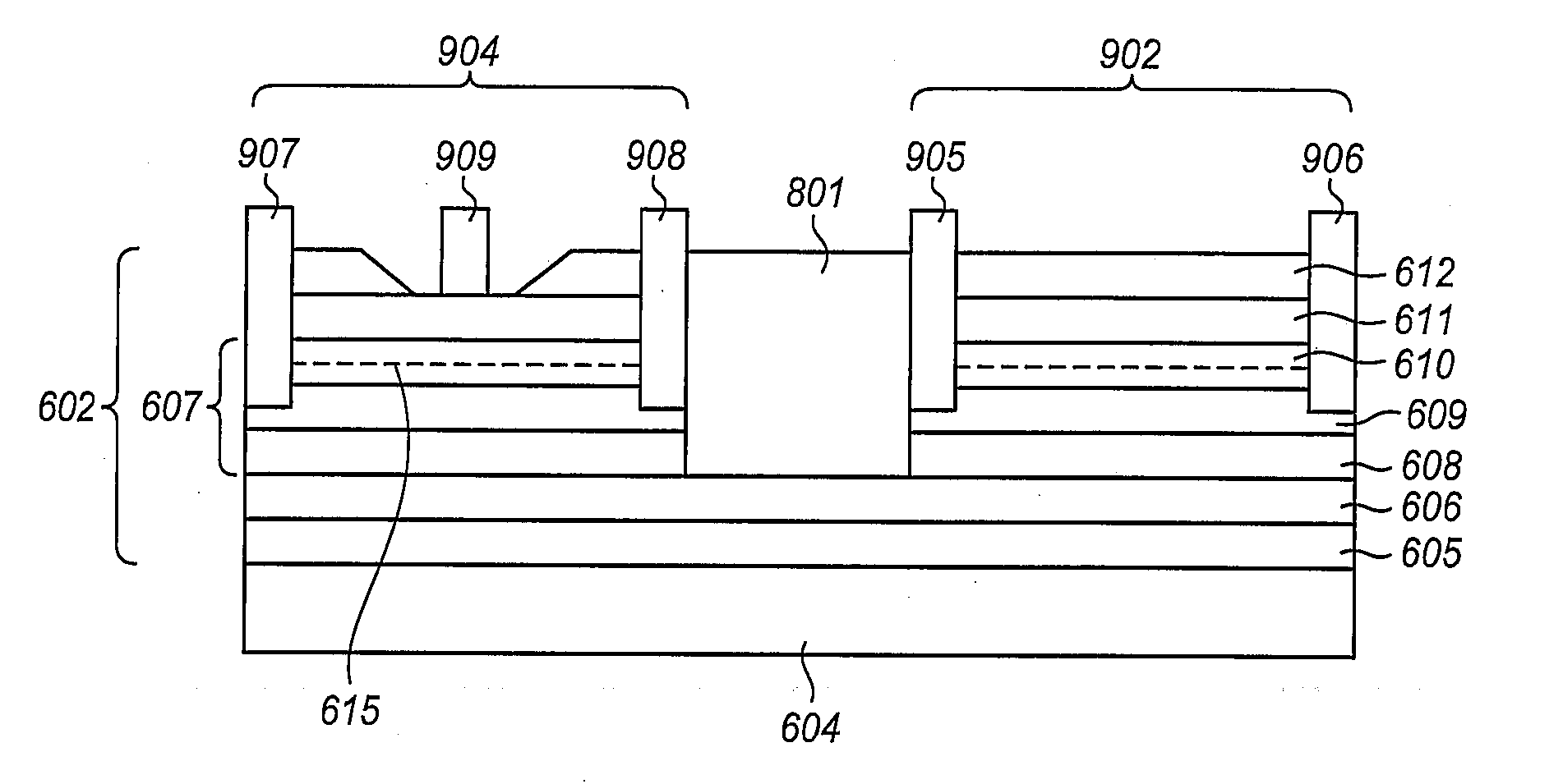
[0026]FIG. 1 is an isometric view of an EMR sensor 100 in the prior art. The EMR sensor 100 includes an EMR structure 102 that is a III-V heterostructure formed on a semiconducting substrate 104, such as GaAs. EMR sensor 100 may alternatively be formed on a basis of silicon or germanium. The EMR structure 102 is a mesa above substrate 104 that results from a subtractive process, such as reactive ion etching (RIE), ion milling, or wet etching. The EMR structure 102 includes a first barrier layer 106 of semiconducting material having a first band gap, a layer 107 of semiconducting material for the channel formed on top of the first barrier layer 106 and having a second band gap smaller than the first band gap, and a second barrier layer 108 of semiconducting material formed on top of layer 107 and having a third band gap greater than the second band gap. The materials in the first barrier layer 106 and the second barrier layer 108 may be similar or id...


PUM

PropertyMeasurementUnit
resistanceaaaaaaaaaa
impedanceaaaaaaaaaa

Abstract

Magnetic sensing chips and methods of fabricating the magnetic sensing chips are disclosed. A magnetic sensing chip as described herein includes an EMR sensor formed on a substrate from multiple semiconductor layers. One or more of the semiconductor layers form a quantum well comprising a two-dimensional electron gas (2DEG) or hole gas (2DHG). The magnetic sensing chip also includes one or more transistors formed on the substrate from the multiple semiconductor layers. The transistor(s) likewise include a quantum well comprising a 2DEG or 2DHG. The EMR sensor and the transistor(s) are connected by one or more connections so that the transistor(s) amplifies data signals from the EMR sensor.

Description

BACKGROUND OF THE INVENTION [0001]1. Field of the Invention[0002]The invention is related to the field of magnetic sensing systems and, in particular, to fabricating a magnetic sensing chip having an extraordinary magnetoresistive (EMR) sensor and one or more transistors formed on the same substrate.[0003]2. Statement of the Problem[0004]A magnetoresistive (MR) read element based on extraordinary magnetoresistance (EMR) effect has been proposed for magnetic recording hard disk drives. Read elements based on EMR include an EMR sensor. The advantage of an EMR sensor over conventional giant magnetoresistive (GMR) sensors and tunneling magnetoresistive (TMR) sensors is that EMR is based on the Lorentz force, similar to devices based on the Hall effect. Thus, EMR sensors utilize nonmagnetic semiconducting materials rather than magnetic metals to detect magnetic fields, and therefore EMR sensors do not suffer from the problem of thermal magnetic noise or spin-torque noise.[0005]An EMR sen...

Claims


Application Information

Patent Timeline
Patent Type & Authority Applications(United States)
IPC IPC(8): G11B5/33
CPCG11B5/3993
Inventor FOLKS, LIESLFONTANA, ROBERT E.GURNEY, BRUCE A.KLAASSEN, KLAAS B.MAAT, STEFAN
Owner WESTERN DIGITAL TECH INC
Why Eureka
Try Eureka