Bottom electrode for MRAM device and method to fabricate it

a technology of mram device and bottom electrode, which is applied in the direction of magnetic field-controlled resistors, digital storage, instruments, etc., can solve the problems of limiting the further reduction of line width, ic device cannot be made very high density, and electrical shorting problems, so as to minimize any possible surface damage to said substrate

Active Publication Date:
View PDF9 Cites 27 Cited by
  • Summary
  • Abstract
  • Description
  • Claims
  • Application Information

AI Technical Summary

Benefits of technology

[0018]It has been an object of at least one embodiment of the present invention to provide a process for forming a bottom electrode for an MTJ stack on a silicon nitride substrate in such a way as to minimize any possible surface damage to said substrate.

Problems solved by technology

However, vertical features created by IBE always have an extended slope on the edge, which not only could creates electrical shorting problems but also limits further reduction of line width and make it impossible to make very high density IC device.
In general, RIE is considered a better approach to creating well-defined three dimensional micro-features but there are several major problems currently associated with the RIE process:
(2) This etching process always results in a large amount of re-deposition all over the surface of the device due to the non-volatility of the reaction products.
This not only affects the MTJ's overall dimensions, but also results in serious damage to the edge of the MTJ's tunnel barrier layer.

Method used


Image

  • Bottom electrode for MRAM device and method to fabricate it
  • Bottom electrode for MRAM device and method to fabricate it
  • Bottom electrode for MRAM device and method to fabricate it

Examples


first embodiment

[0040]For the first embodiment, as an alternative to the use of NiCr as a ‘glue’ layer, a special treatment of the SiN substrate surface may be used instead:

Sputter-clean SiN / OSURu30 / α-Ta120 / TaN150

[0041]where OSL stands for oxygen surfactant layer. When OSL is used to treat the SiN surface, SiOxyNitride / RuO is formed at the SiN / Ru interface which then promotes good adhesion.

[0042]We now provide a description of the processes used to manufacture the two embodiments of the invention:

1st embodiment

1st Embodiment

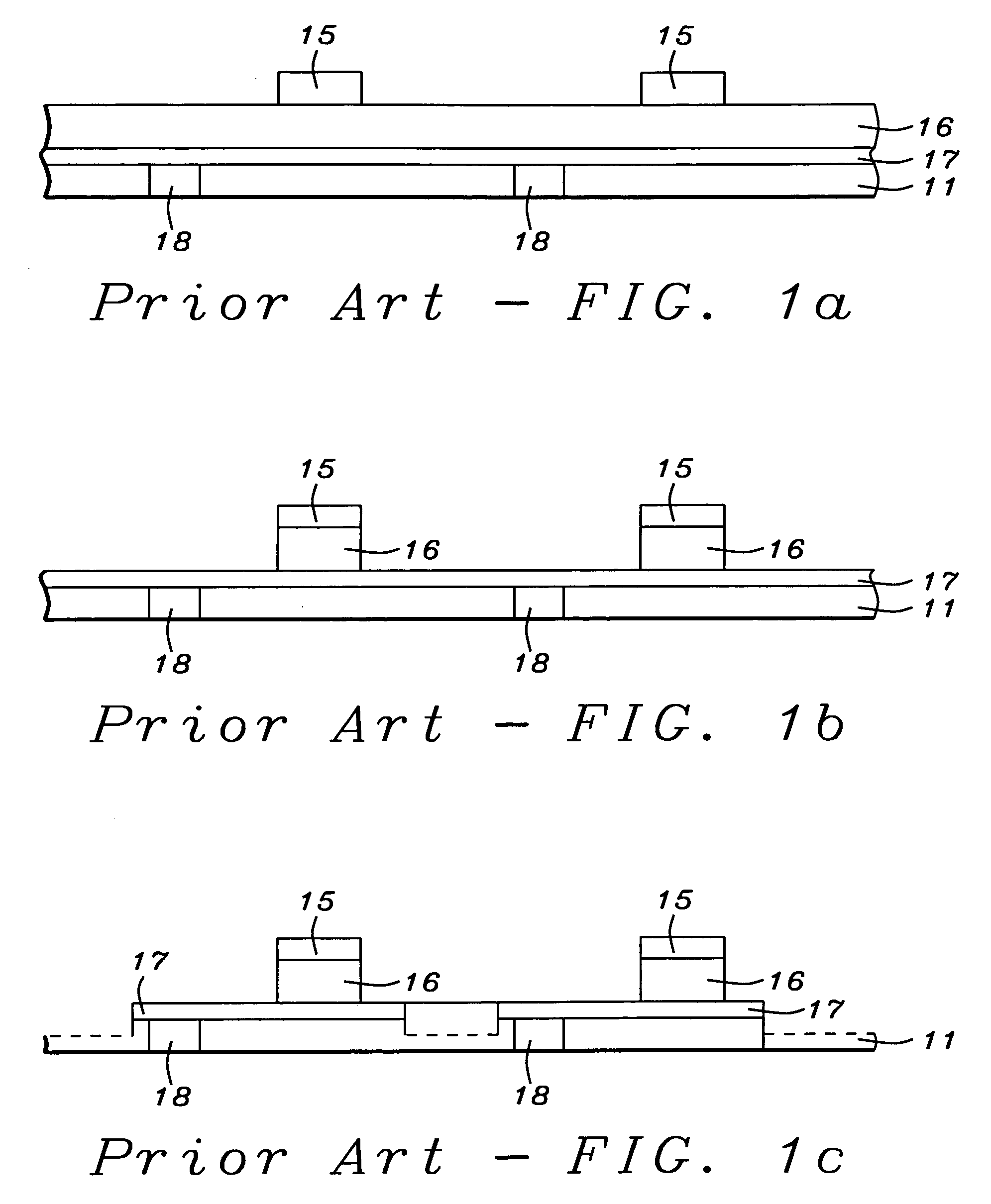
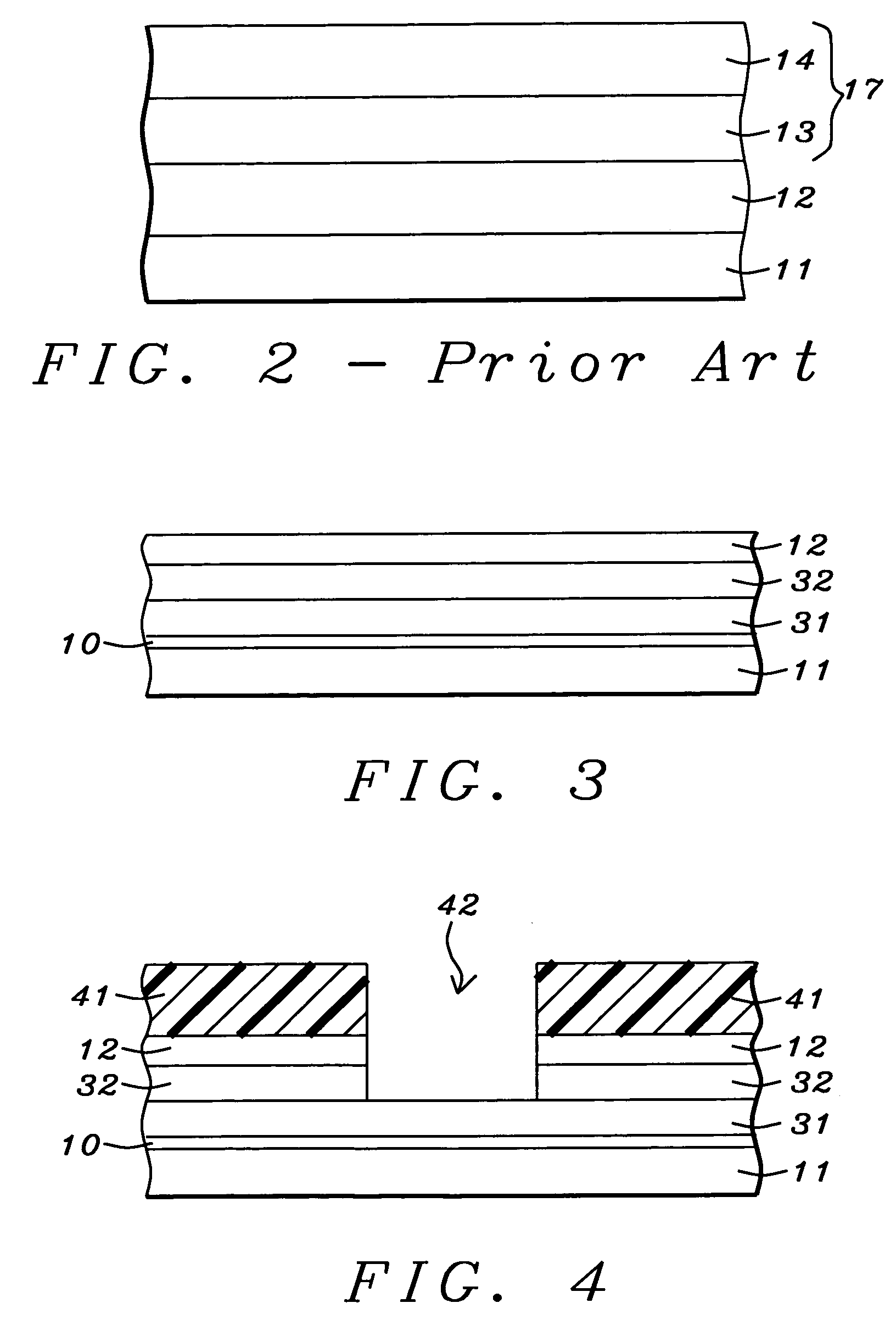
[0043]Referring now to FIG. 3, the process starts with sputter cleaning of the surface of substrate layer 11, followed by depositing thereon layer of NiCr 10 onto which is deposited ruthenium layer 31 to a thickness between about 20 and 30 Angstroms. This is followed by the deposition, to a thickness between about 100 and 200 Angstroms, of alpha tantalum layer 32 (on ruthenium layer 31). Next, tantalum nitride layer 12 is deposited on layer of alpha tantalum 32 (to a thickness between about 100 and 150 Angstroms).

[0044]Now follows a key feature of the invention which is the process used to etch the bottom electrode sheet (layers 12 / 32 / 31 / 11) into individual bottom electrodes without, at the same time, significantly penetrating silicon nitride substrate 11. This is accomplished in two main steps, as follows:

[0045]Referring now to FIG. 4, photoresist mask 41, that defines the required multiple electrode shapes, is formed on the upper surface of layer 12. Then, a first re...

2nd embodiment

2nd Embodiment

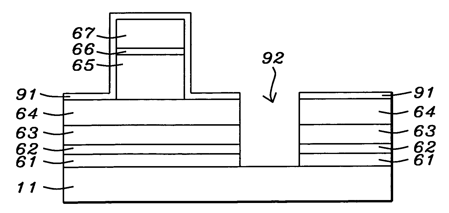
[0047]Referring now to FIG. 6, the process of the 2nd embodiment starts with sputter cleaning of the surface of SiN substrate layer 11 onto which is deposited layer of tantalum nitride 61 to a thickness between about 20 and 30 Angstroms. This is immediately followed by the deposition (onto the top surface of 61) of layer 62 of NiCr to a thickness between about 20 and 30 Angstroms. Note that it is critical for the effectiveness of this embodiment that layers 61 and 62 always be used together. The motivation for this is the excellent adhesion of TaN to SiN, the excellent adhesion of NiCr to TaN, and the excellent adhesion of Ru to NiCr. Furthermore, NiCr is an effective seed layer for Ru so it also serves to minimize the resistivity of Ru layer 63.

[0048]Next, layer 63 of ruthenium is deposited on layer 62 and then alpha tantalum layer 64 is deposited on ruthenium layer 63. Layers 61-64 now constitute a base layer on which MTJ devices can be formed. Seen in FIG. 6 are pin...


PUM

PropertyMeasurementUnit
thicknessaaaaaaaaaa
thicknessaaaaaaaaaa
thicknessaaaaaaaaaa

Abstract

Formation of a bottom electrode for an MTJ device on a silicon nitride substrate is facilitated by including a layer of ruthenium near the silicon nitride surface. The ruthenium is a good electrical conductor and it responds differently from Ta and TaN to certain etchants. Adhesion to SiN is enhanced by using a TaN/NiCr bilayer as “glue”. Thus, said included layer of ruthenium may be used as an etch stop layer during the etching of Ta and/or TaN while the latter materials may be used to form a hard mask for etching the ruthenium without significant corrosion of the silicon nitride surface.

Description

[0001]This application is related to HT05-013, filed on ______ as application Ser. No. ______ and is herein incorporated, by reference, in its entirety.FIELD OF THE INVENTION[0002]The invention relates to the general field of magnetic tunnel junctions (MTJs) with particular reference to the bottom electrode located between them and the inter-layer dielectric (ILD) of an integrated circuit.BACKGROUND OF THE INVENTION[0003]Magnetoresistive Random Access Memory (MRAM), based on the integration of silicon CMOS with Magnetic Tunnel Junction (MTJ)s, is a major emerging technology, highly competitive with existing semiconductor memories (SRAM, DRAM, Flash etc). The MTJ consists of two ferromagnetic layers separated by a thin dielectric layer. Magnetization of the two ferromagnetic layers can be arranged to be in either parallel (low resistance) or anti-parallel (high resistance) magnetization states, representing “1” and “0” respectively, The MTJ memory cells are usually inserted at the ba...

Claims


Application Information

Patent Timeline
Patent Type & Authority Applications(United States)
IPC IPC(8): H01L21/00
CPCH01L43/12H01L43/08G11C11/161H10N50/10H10N50/01
Inventor XIAO, RONGFUHORNG, CHENG T.TONG, RU-YINGTORNG, CHYU-JINHZHONG, TOMKULA, WITOLDKO, TERRY KIN TINGCAO, WEIKAN, WAI-MING J.HONG, LIUBO
Why Eureka
Try Eureka