

Method and structure for thin film photovoltaic materials using bulk semiconductor materials
a photovoltaic material and semiconductor technology, applied in the field of photovoltaic materials, can solve the problems of reducing the processing efficiency of thin films, so as to improve the processing efficiency, facilitate the use, and improve the effect of conversion efficiency
- Summary
- Abstract
- Description
- Claims
- Application Information
AI Technical Summary
Benefits of technology
Problems solved by technology
Method used
Image

Examples
example 1
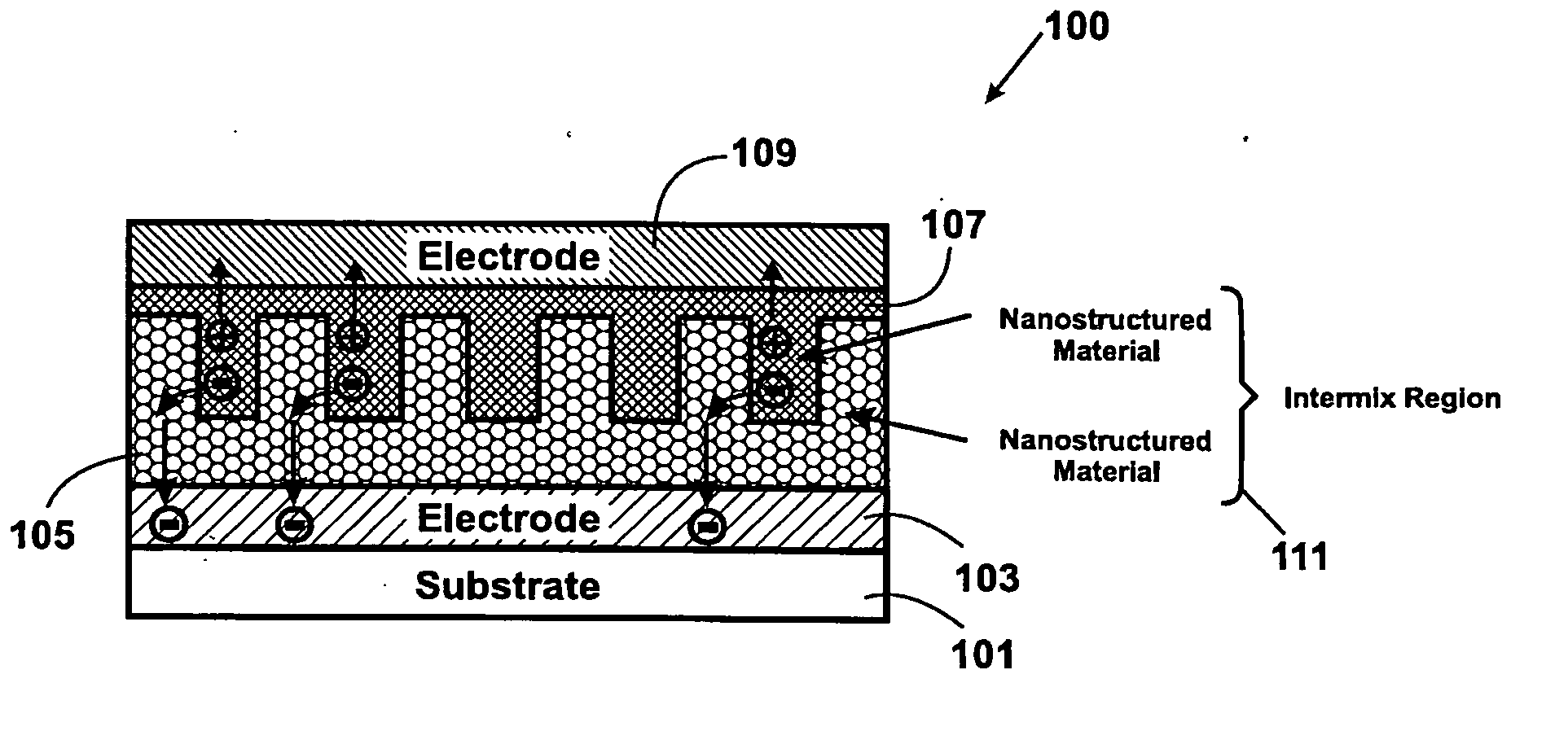
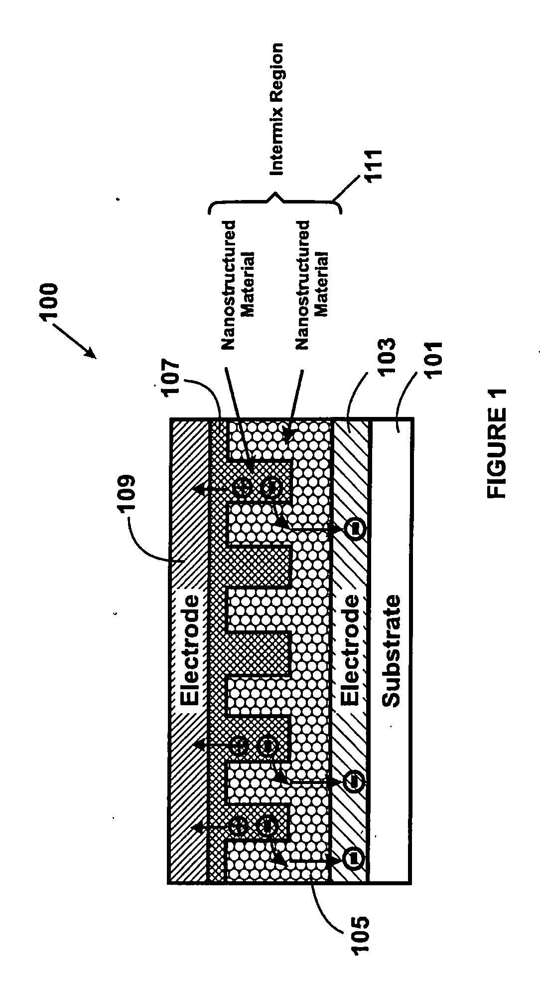
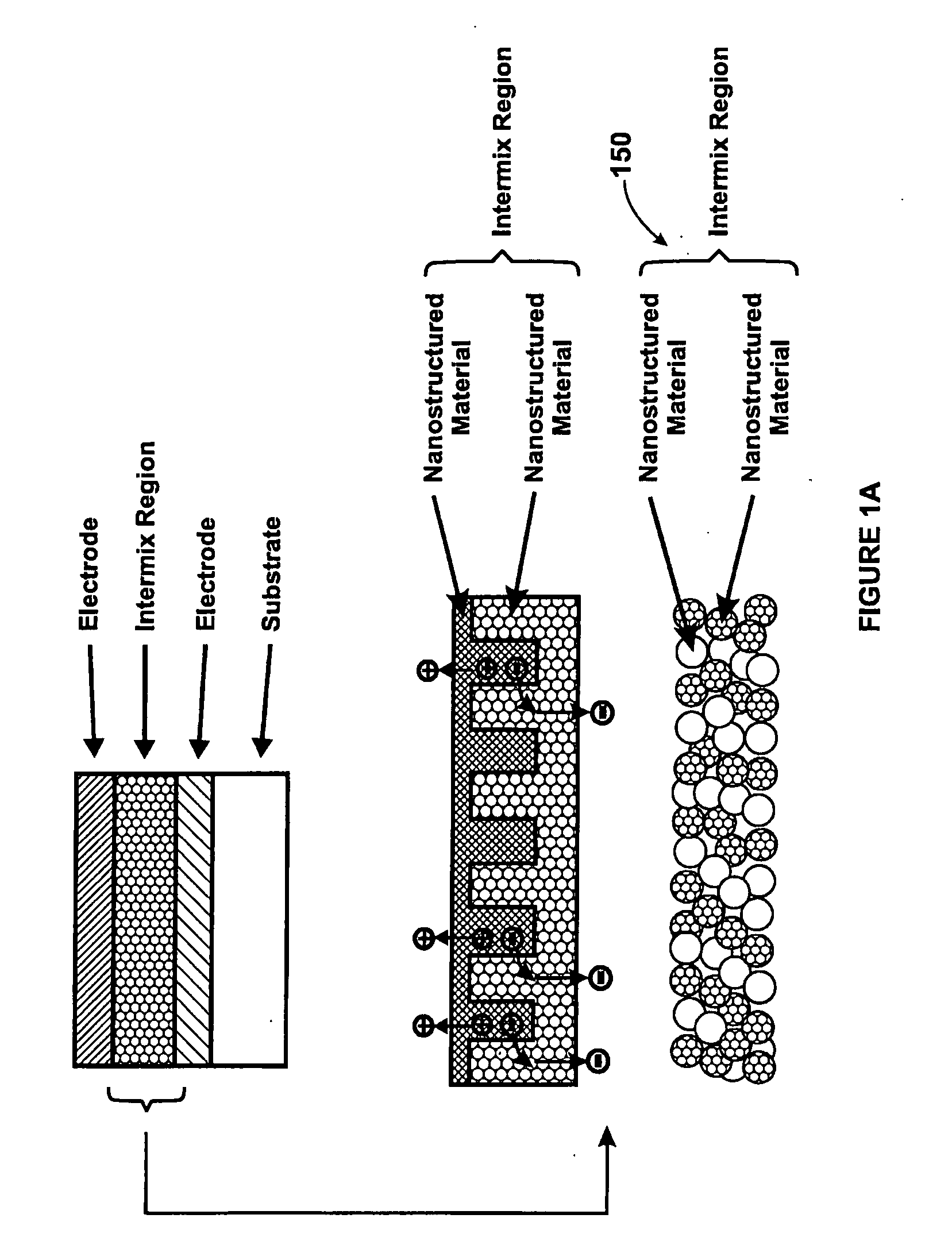
[0385] On a substrate, which can be any optically clear material such as glasses, fused silica, plastic, etc., a transparent conducting electrode (TCE) is deposited, which can be performed with a variety of vacuum methods such as sputtering, evaporation, and solution deposition methods. Examples of TCEs are indium tin oxide (ITO), zinc oxide doped with Al (ZnO:Al), and tin oxide doped with fluorine (SnO2:F). In these examples, we use ZnO:Al.
[0386] A layer of nanoparticles (NPs) of a first material is then deposited on the TCE. The thickness of this film can range from about 50 nm to about 1000 nm. This is performed using a colloidal suspension of the NPs and with various types of solution deposition processes such as spin coating, spraying, ink jet printing, dipping, doctor blading, electrophoresis, electrochemical deposition, etc. The first material deposited can be metal oxides such as ZnO, TiO2, SnO2, WO3, Fe2O3, etc. Alternatively, the first material can be metal sulfide such a...
example 2
[0389] In another embodiment of Example 1, NPs of the first material and NPs of the second material are deposited together in a fashion similar to the deposition of NPs of the first material in Example 1. As in Example 1, both are then sintered for the specified time and temperature or by applying pressure.
example 3
[0390] Begin with the TCE coated substrate of Example 1. A film of electron transporting hole blocking material (ETHBM) is deposited using vacuum techniques such as sputtering or evaporation or solution deposition techniques with a thickness ranging from about 100 nm to about 1000 nm. The ETHBM can be metal oxides such as ZnO, TiO2, SnO2, WO3, Fe2O3, etc, and can be undoped or n-doped. The nanocomposite film described in Example 1 is then processed on the ETHBM. Finally, a top electrode is deposited on the nanocomposite film. This top electrode can be deposited by methods such as sputtering, evaporation, screen printing, painting, foil lamination, etc.
PUM
 Abstract
Description
Claims
Application Information