Nitride semiconductor device

Active Publication Date: 2008-04-24
KK TOSHIBA
View PDF11 Cites 132 Cited by
  • Summary
  • Abstract
  • Description
  • Claims
  • Application Information

AI Technical Summary

Benefits of technology

[0029] The present invention has been made in view of these circumstances, and an object thereof is to provide a nitride semiconductor device in which the threshold voltage can be controlled e

Problems solved by technology

As a result, the on-resistance becomes low.
In other words, as for the nitride semiconductor device according to the first reference art, it is difficult to fabricate a normally-off type nitride semiconductor device having low on-resistance with a high yield.
Because of the problem of the processing precision, however, there is a problem that it is difficult to fabricate the normally-off type semiconductor device with a high yield.
It is known that use of dry etching such as the RIE method on the nitride causes introduction of etching damages due to the nitrogen vacancy into the semiconductor device.
When processing the above-described recess structure, therefore, etching damage is introduced into a gate recess region and the channel mobility of the two-dimensional electron system under the gate recess is reduced, and it is difficult to fabricate a semiconductor device having low on-resistance.
Therefore, there is also a problem that it is difficult to fabricate a nitride semiconductor device by controlling the threshold voltage with a high yield.
However, the third reference art has the same problem as the second reference art does.
Because of the problem of the processing precision, the

Method used


Image

  • Nitride semiconductor device
  • Nitride semiconductor device
  • Nitride semiconductor device

Examples


Example

First Embodiment

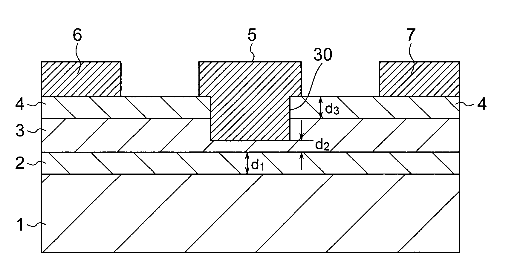
[0065]FIG. 1 is a sectional view schematically showing a structure of a nitride semiconductor device according to a first embodiment of the present invention. The nitride semiconductor device has a configuration obtained by successively stacking a carrier transit layer 1 formed of a non-doped nitride semiconductor AlXGa1-XN (0≦X2 formed of a non-doped or n-type nitride semiconductor AlYGa1-YN (01, a threshold control layer 3 formed of a non-doped or n-type nitride semiconductor having a lattice constant equal to that of the carrier transit layer 1, and a carrier induction layer 4 formed of InWAlZGa1-W-ZN (05 is formed, a recess structure 30 is formed by removing the whole of the carrier induction layer 4 and a part of the threshold control layer 3. A gate electrode 5 is formed so as to cover the recess structure 30. A source electrode 6 and a drain electrode 7 are formed in substantially symmetrical positions on the carrier induction layer 4 with the gate electrode ...

Example

Second Embodiment

[0096] A nitride semiconductor device according to a second embodiment of the present invention is shown in FIG. 16. The nitride semiconductor device according to the present embodiment has a configuration obtained from the first embodiment shown in FIG. 1 by providing an insulation film 8 so as to cover the carrier induction layer 4, the gate electrode 5, the source electrode 6 and the drain electrode 7 and providing a field plate electrode 9 on the insulation film 8 so as to overlap the gate electrode 5, the source electrode 6, and the carrier induction layer 4 between the gate electrode 5 and the source electrode 6.

[0097] The field plate electrode 9 is formed to extend from its first end on the insulation film 8 on a side having the source electrode 6 under, to its second end A located on the drain electrode 7 side as compared with an end B of the gate electrode 5 on the carrier induction layer 4 on the drain electrode 7 side (the right side in FIG. 16). In FIG...

Example

Third Embodiment

[0100] A nitride semiconductor device according to a third embodiment of the present invention is shown in FIG. 17. The nitride semiconductor device according to the present embodiment has a configuration obtained from the first embodiment shown in FIG. 1 by providing a gate insulation film 10 on the bottom face and side faces of the recess structure 30 and on the carrier induction layer 4 between the gate electrode 5 and the source electrode 6 and between the gate electrode 5 and the drain electrode 7. In other words, the nitride semiconductor device according to the present embodiment has a configuration in which the gate electrode 5 is formed in the recess structure 30 via the gate insulation film 10. Preferably, a SiN film which is reported to have a low interface level with an AlGaN film is used as the gate insulation film 10. For controlling the threshold voltage, the gate electrode 5 needs only to be located over the threshold control layer 3 and it is not ne...


PUM


Abstract

A nitride semiconductor device includes: a first nitride semiconductor layer formed of non-doped AlxGa1-XN (0≦X<1); a second nitride semiconductor layer formed on the first nitride semiconductor layer of non-doped or n-type AlYGa1-YN (0<Y≦1, X<Y), and having a smaller lattice constant than that of the first nitride semiconductor layer; a third nitride semiconductor layer formed on the second nitride semiconductor layer of a non-doped or n-type nitride semiconductor, and having a lattice constant equal to that of the first nitride semiconductor layer; a fourth nitride semiconductor layer formed on the third nitride semiconductor layer of InWAlZGa1-W-ZN (0<W≦1, 0<Z<1); a gate electrode formed in a recess structure having a bottom face which arrives at the third nitride semiconductor layer; and a source electrode and a drain electrode.

Description

CROSS-REFERENCE TO RELATED APPLICATION [0001] This application is based upon and claims the benefit of priority from prior Japanese Patent Application No. 2006-286332 filed on Oct. 20, 2006 in Japan, the entire contents of which are incorporated herein by reference. BACKGROUND OF THE INVENTION [0002] 1. Field of the Invention [0003] The present invention relates to a nitride semiconductor device. [0004] 2. Related Art [0005] In a power semiconductor device such as a switching element or a high frequency power semiconductor device, it is effective to use a material having a high critical electric field and consequently a nitride semiconductor material having high critical electric field strength is used. [0006] As for a conventional nitride semiconductor device using a nitride semiconductor material, a first reference art is known. According to the first reference art, a carrier transit layer formed of an AlXGa1-XN (0≦X<1) film and a barrier layer formed of an AlYGa1-YN (0<Y≦1,...

Claims


Application Information

Patent Timeline
IPC IPC(8): H01L29/778
CPCH01L29/2003H01L29/205H01L29/66462H01L29/802H01L29/7785H01L29/7787H01L29/861H01L29/7781
Inventor KURAGUCHI, MASAHIKO
Owner KK TOSHIBA
Why Eureka
Try Eureka