Method of manufacturing a semiconductor integrated circuit device

a manufacturing method and integrated circuit technology, applied in the direction of individual semiconductor device testing, semiconductor/solid-state device testing/measurement, instruments, etc., can solve the problems of increasing the number of test pads, reducing the area of test pads, and difficult to align the probes with the arrangement positions of test pads

Active Publication Date: 2008-04-24
RENESAS ELECTRONICS CORP
View PDF8 Cites 5 Cited by
  • Summary
  • Abstract
  • Description
  • Claims
  • Application Information

AI Technical Summary

Benefits of technology

[0017]Since a contact area between the membrane sheet and the pressing member in contact with the sheet can be as small as possible, even when foreign matter is at

Problems solved by technology

For this reason, this leads not only to an increase in number of test pads (bonding pads), but also to a narrow-pitch arrangement of the test pads, which reduces the area of the test pad.
When a prober with cantilever-like probes is intend

Method used


Image

  • Method of manufacturing a semiconductor integrated circuit device
  • Method of manufacturing a semiconductor integrated circuit device
  • Method of manufacturing a semiconductor integrated circuit device

Examples


Embodiment Construction

[0057]The terms as used in the present application have the following means, which are explained below before the invention is described in detail.

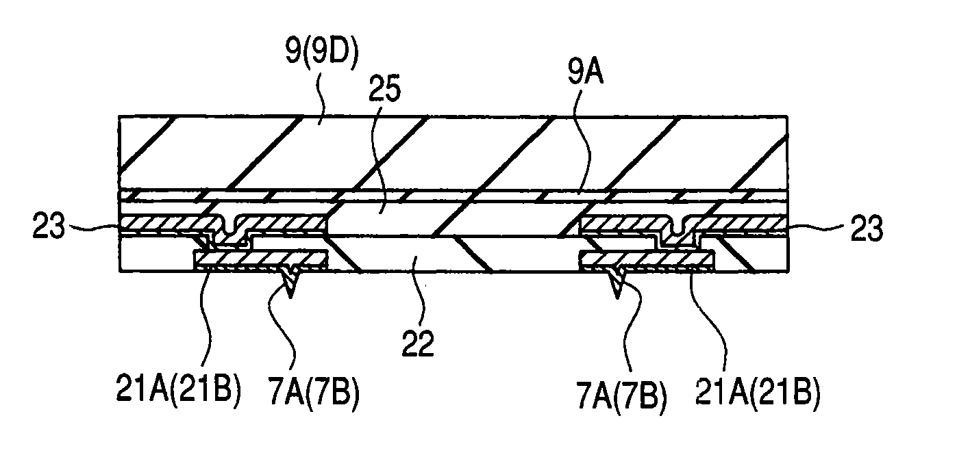
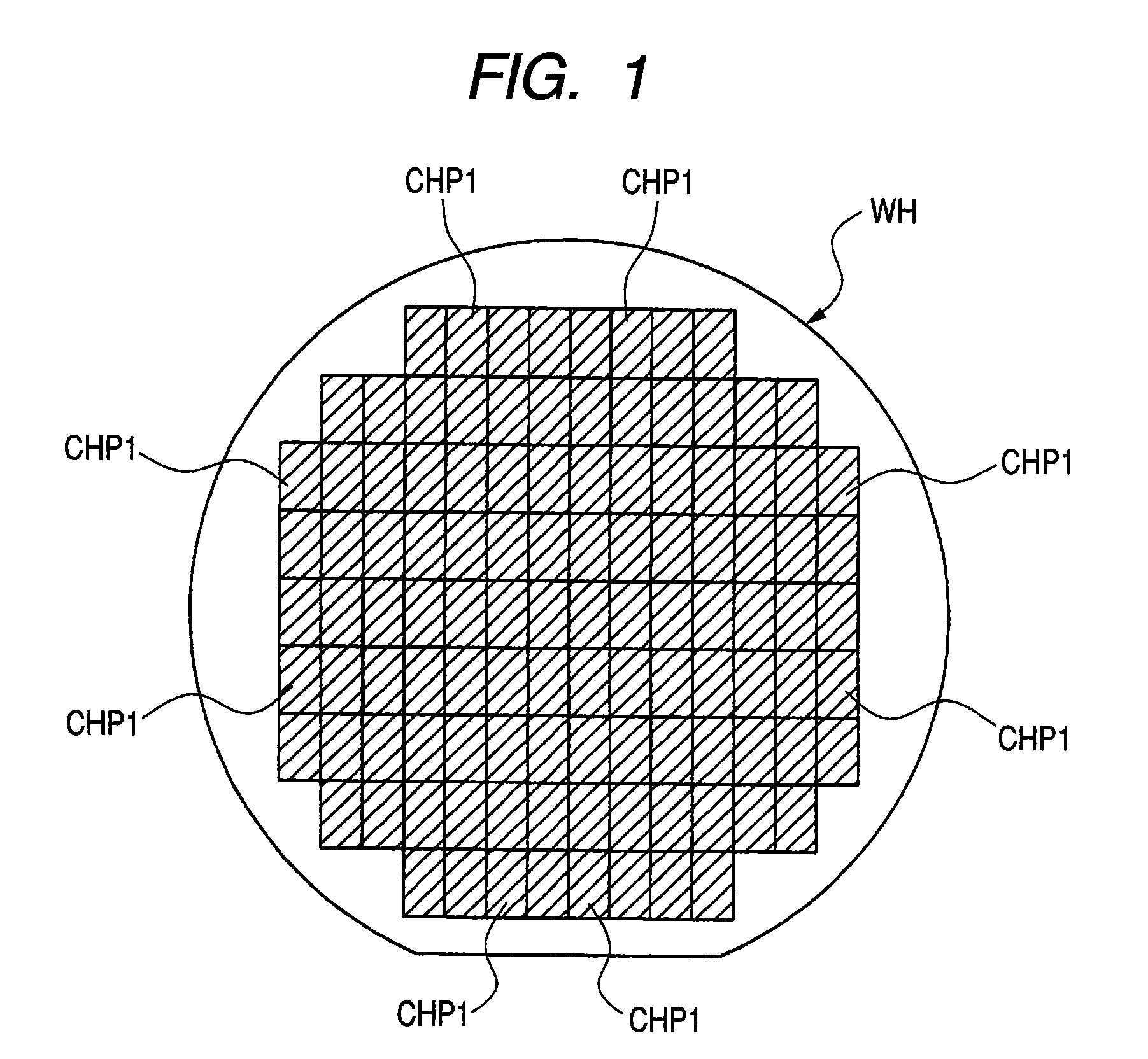
[0058]The term “wafer” as used herein includes a single-crystal silicon substrate (in general, having a substantially disk-like shape) used for manufacturing of integrated circuits, a silicon on insulator (SOI) substrate, an epitaxial substrate, a sapphire substrate, a glass substrate, other insulating, semi-insulating or semiconductor substrates, and a composite substrate thereof. Unless otherwise specified, the term “semiconductor integrate circuit device” as used herein may include not only a semiconductor integrated circuit formed on a semiconductor or insulating substrate, such as a silicon wafer or a sapphire substrate, but also a semiconductor integrated circuit, such as a TFT (Thin Film Transistor) or STN (Super-Twisted-Nematic) liquid crystal, formed on another insulating substrate, such as glass.

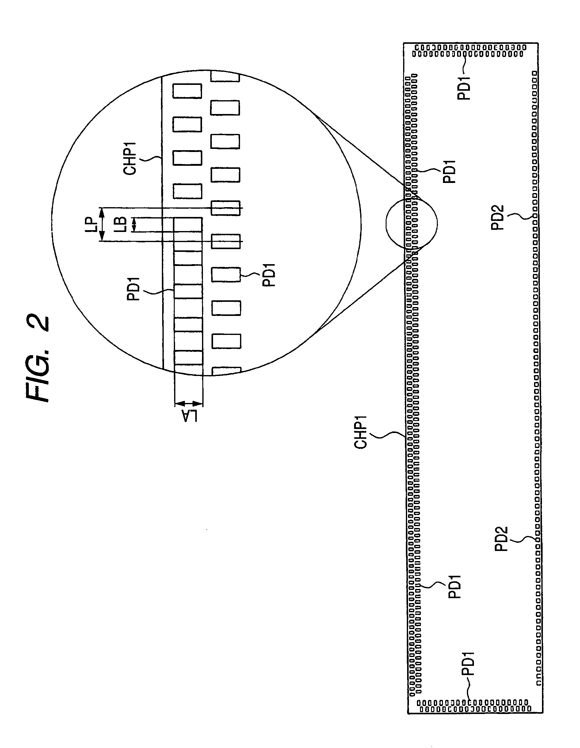
[0059]The term “device surface” a...


PUM


Abstract

A technique of manufacturing a semiconductor integrated circuit device is provided for reducing the possibility of attachment of foreign matter to a membrane probe when performing probe inspection using the membrane probe formed by the manufacturing technique. A pressing member for pressing a membrane sheet includes a pressing pin receiving portion relatively disposed above for receiving the tip of a pressing pin of the plunger in a recess, and a membrane sheet pressing portion relatively disposed below. The membrane sheet pressing portion in contact with the membrane sheet has the minimum plane size to enable pressing of the entire surface of one chip of interest to be subjected to the probe inspection.

Description

CROSS-REFERENCE TO RELATED APPLICATIONS[0001]The disclosure of Japanese Patent Application No. 2006-288642 filed on Oct. 24, 2006 including the specification, drawings and abstract is incorporated herein by reference in its entirety.BACKGROUND OF THE INVENTION[0002]The present invention relates to a manufacturing technique of a semiconductor integrated circuit device, and more particularly, to a technique that is effectively applied to electric inspection of a semiconductor integrated circuit by pressing probes of a probe card against electrode pads of the semiconductor integrated circuit device.[0003]Japanese Unexamined Patent Publication No. 2005-24377 (Patent Document 1) and Japanese Unexamined Patent Publication No. 2004-144742 (Patent Document 2) disclose a prober structure including probe needles, an insulating film, and wiring for deriving which are formed using a manufacturing technique of a semiconductor integrated circuit device, a pushing block, and a spring probe. A coni...

Claims


Application Information

Patent Timeline
IPC IPC(8): H01L21/66
CPCH01L22/34H01L2924/0002H01L2924/00H01L22/00
Inventor HASEBE, AKIOMOTOYAMA, YASUHIRONARIZUKA, YASUNORINAKAMURA, SEIGO
Owner RENESAS ELECTRONICS CORP
Why Eureka
Try Eureka