Semiconductor integrated circuit device

a technology of integrated circuit and semiconductor, which is applied in the direction of instant pulse delivery arrangement, battery arrangement, pulse manipulation, etc., can solve the problems of large current consumption, large chip size of ic b>1/b>, and significant decrease in the capacity of secondary cells, so as to reduce current consumption and reduce chip size

Inactive Publication Date: 2008-05-01
DENSO CORP
View PDF7 Cites 40 Cited by
  • Summary
  • Abstract
  • Description
  • Claims
  • Application Information

AI Technical Summary

Benefits of technology

[0009]In view of the above-described problem, it is an object of the present invention to provide a semiconductor integrated c

Problems solved by technology

If the secondary cell is used outside its rated voltage range, capacity of the secondary cell significantly decreases, an

Method used


Image

  • Semiconductor integrated circuit device
  • Semiconductor integrated circuit device
  • Semiconductor integrated circuit device

Examples


first embodiment

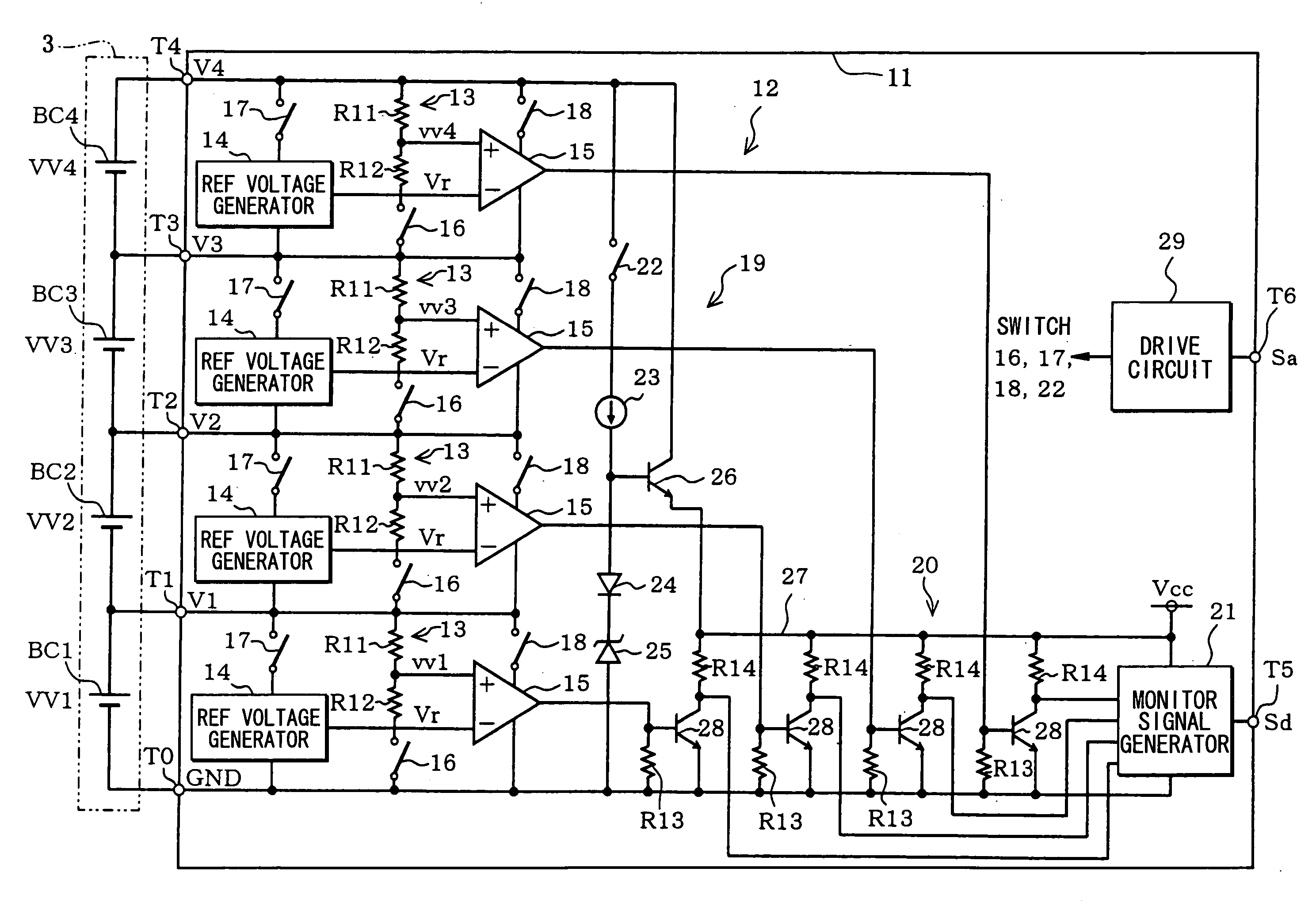
[0028]Referring to FIG. 1, an integrated circuit (IC) 11 according to a first embodiment of the present invention includes a cell voltage monitor circuit 12 that monitors cell voltages VV1-VV4 of secondary cells BC1-BC4 connected in series. The cells BC1-BC4 construct an assembled battery 3. For example, the assembled battery 3 is used as a battery for an electric vehicle (HEV) and a hybrid electric vehicle (HEV). The secondary cells BC1-BC4, may be for example, lithium ion cells. The IC 11 has input terminals T0-T4 and output terminals T5, T6. The cell BCi is connected between the input terminals T1-1, T1, where i is an integer from 1 to 4. For example, the cell BC2 is connected between the input terminals T1, T2.

[0029]When at least one of the cell voltages VV1-VV4 of the cells BC1-BC4 exceeds a predetermined reference voltage, a monitor signal Sd having a first level (e.g., high level) is outputted from the output terminal T5 of the IC 11. Further, when an interruption signal Sa (...

second embodiment

[0047]An IC 37 according to a second embodiment of the present invention is described with reference to FIG. 3. Differences between the IC 37 shown in FIG. 3 and the IC 11 shown in FIG. 1 are as follows:

[0048]A comparator 15 provided to a cell BC1 is powered by a voltage supplied via a switch 18 from between positive and negative terminals of the cell BC1. The cell BC1 is arranged on the lowest potential side of the assembled battery 3. The comparator 15 provided to the cell BCi is powered by a voltage supplied via a switch 18 from between a positive terminal of a cell BCi and a negative terminal of a cell BCi-1, where i is an integer from 2 to 4. For example, the comparator 15 provided to the cell BC3 is powered by a voltage supplied via a switch 18 from between a positive terminal of the cell BC3 and a negative terminal of the cell BC2.

[0049]In such an approach, even when the cell voltages VV1-VV4 decrease significantly, the comparison circuit 15 provided to each of the cells CB2-...

third embodiment

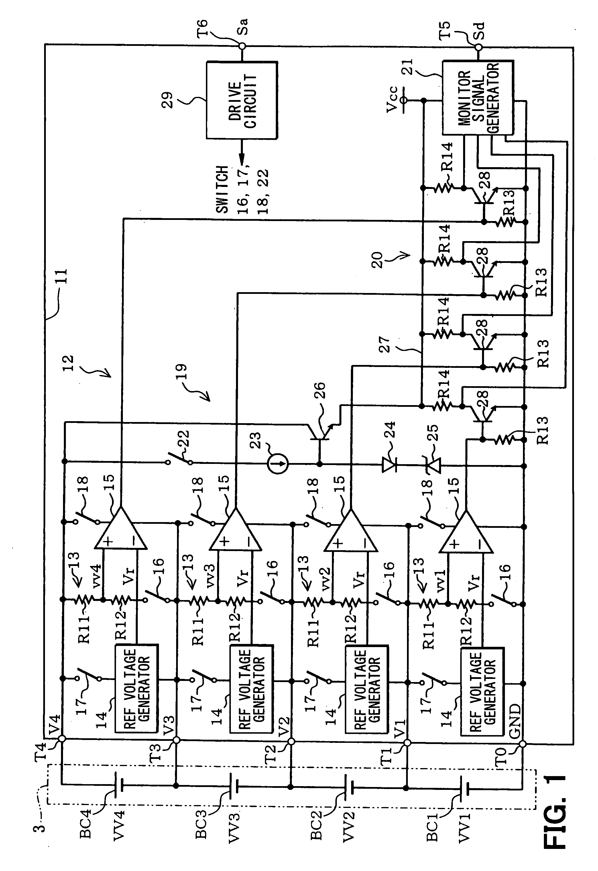
[0052]An IC 11a according to a third embodiment of the present invention is described with reference to FIG. 4. Differences between the IC 11a shown in FIG. 4 and the IC 11 shown in FIG. 1 are as follows:

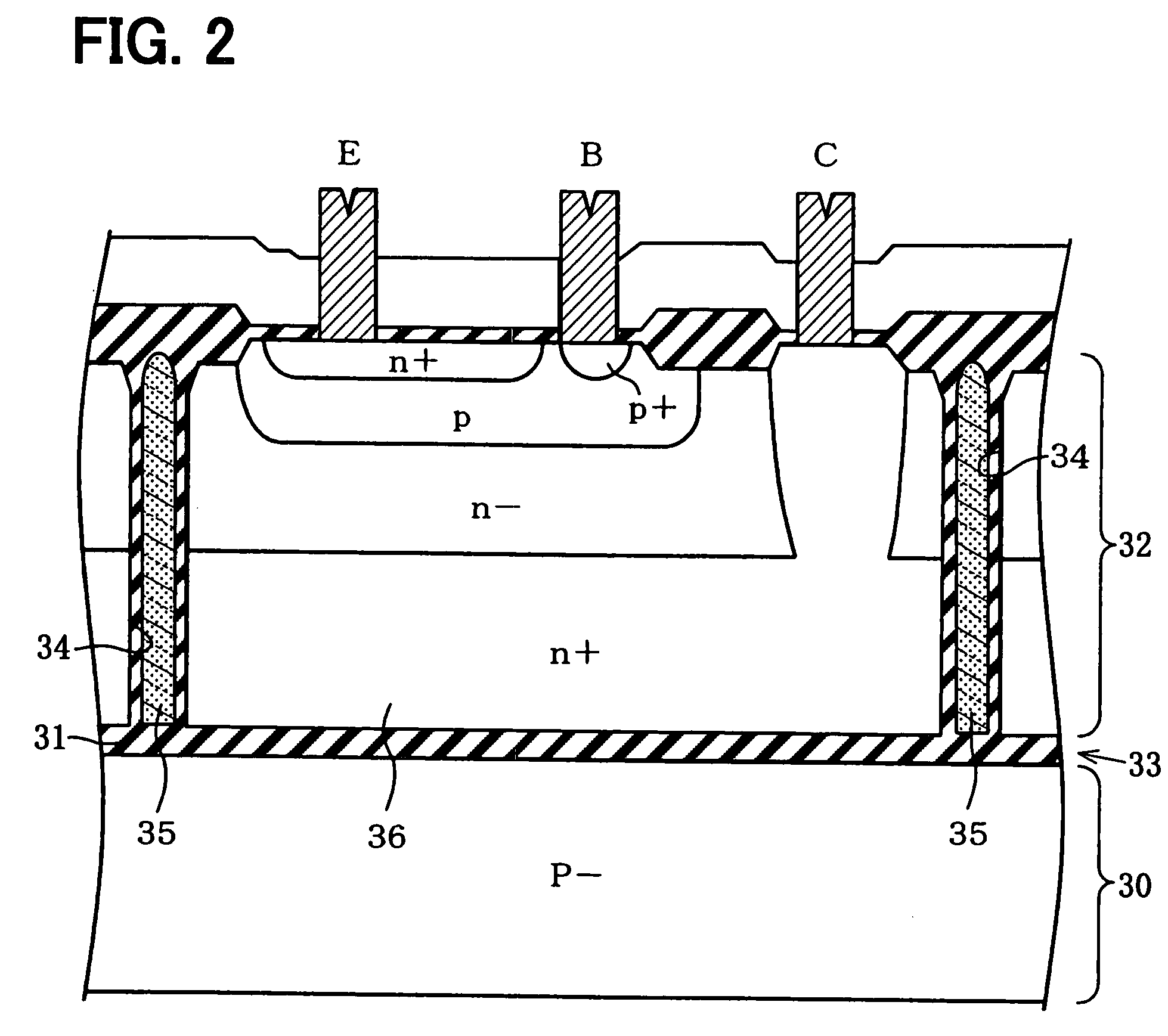
[0053]In the first embodiment, as shown in FIG. 2, each element is electrically isolated by the trench 34 formed on the single crystal silicon layer 32 of the SOI substrate 33.

[0054]Like in the first embodiment, in the third embodiment, each element is electrically isolated by the trench 34 formed on the single crystal silicon layer 32 of the SOI substrate 33. Further, each circuit forming region, where elements operating with respect to the same potential are formed, is electrically isolated by an additional trench. Specifically, as shown in FIG. 4, circuit forming regions, where the sub monitor circuits are formed, respectively, are isolated from each other by the additional trench. Further, a circuit forming region, where the power supply circuit 19, the C / V conversion circuit 20...


PUM


Abstract

A semiconductor integrated circuit device formed by a trench dielectric isolation technique has input terminals connected to positive and negative terminals of secondary cells of an assembled battery and includes monitor circuits for respectively monitoring cell voltages of the cells. Each monitor circuit includes a cell voltage detection circuit, a reference voltage generation circuit, and a comparison circuit. The cell voltage detection circuit divides a voltage between the input terminals connected to the positive and negative terminals of a corresponding cell and detects the cell voltage based on the divided voltage. The reference voltage generation circuit generates a reference voltage from the cell voltage. The comparison circuit is powered by the cell voltage of the corresponding cell and compares the divided voltage with the reference voltage.

Description

CROSS CHECK TO RELATED APPLICATION[0001]This application is based on and incorporates herein by reference Japanese Patent Applications No. 2006-289945 filed on Oct. 25, 2006 and No. 2007-166110 filed on Jun. 25, 2007.FIELD OF THE INVENTION[0002]The present invention relates to a semiconductor integrated circuit device that monitors a cell voltage of an assembled battery.BACKGROUND OF THE INVENTION[0003]An assembled battery has been used as a battery for an electric vehicle (HEV) and a hybrid electric vehicle (HEV). Such an assembled battery is constructed with a number of secondary cells connected in series to produce a high voltage of about between 100 and 400 volts. For example, an assemble battery of 300 volts is constructed with 150 lead cells (2 volts per cell) connected in series, 250 nickel hydride cells (1.2 volts per cell) connected in series, or 80 lithium ion cells (about 3.6 volts per cell) connected in series.[0004]A secondary cell, in particular, a lithium ion cell is ...

Claims


Application Information

Patent Timeline
IPC IPC(8): H02J7/00H01L21/822H03K5/125H01M10/44G01R19/00H02J7/02
CPCG01R19/0084G01R31/3658H01L29/7317Y02T10/7055H02J7/0021H03K5/24H01M10/482B60L2240/547G01R31/396B60L58/18Y02T10/70Y02E60/10H02J7/0013H02J7/0048
Inventor SOBUE, SATOSHI
Owner DENSO CORP
Why Eureka
Try Eureka