

Trap-charge non-volatile switch connector for programmable logic
a non-volatile switch and logic technology, applied in the field of non-volatile memories and configurable logic elements, can solve the problems of increasing processing costs, requiring high voltage for program and erase, and degrading chip performance, so as to reduce the voltage requirement and the effect of high voltag
- Summary
- Abstract
- Description
- Claims
- Application Information
AI Technical Summary
Benefits of technology
Problems solved by technology
Method used
Image

Examples
second embodiment
[0041]In FIG. 8 is shown the present invention. A P-channel transistor 515 is connected to a memory gate storage transistor 516a between a high voltage VMH and a low voltage VML. The storage transistor 516a is nonvolatile trap charge device where the trap charge element 516b is formed by an insulator, for example a nitride film or a nano-crystal film. The connection between the P-channel transistor 515 and the storage transistor 516a forms a node NB, which is connected to a latch 512 through a write control gate 517. The state of the latch 512 controls the on-off state of the logic interconnect transistor, which couples two logic functions 513 and 514 together when the logic interconnect transistor is turned on.
[0042]Continuing to refer to FIG. 8, the write control gate 517 is opened twice in the process of setting the latch 512, first to reset the latch to a high state and second to program the state of the latch. The latch is reset to a high logic state using the precharge transis...
third embodiment
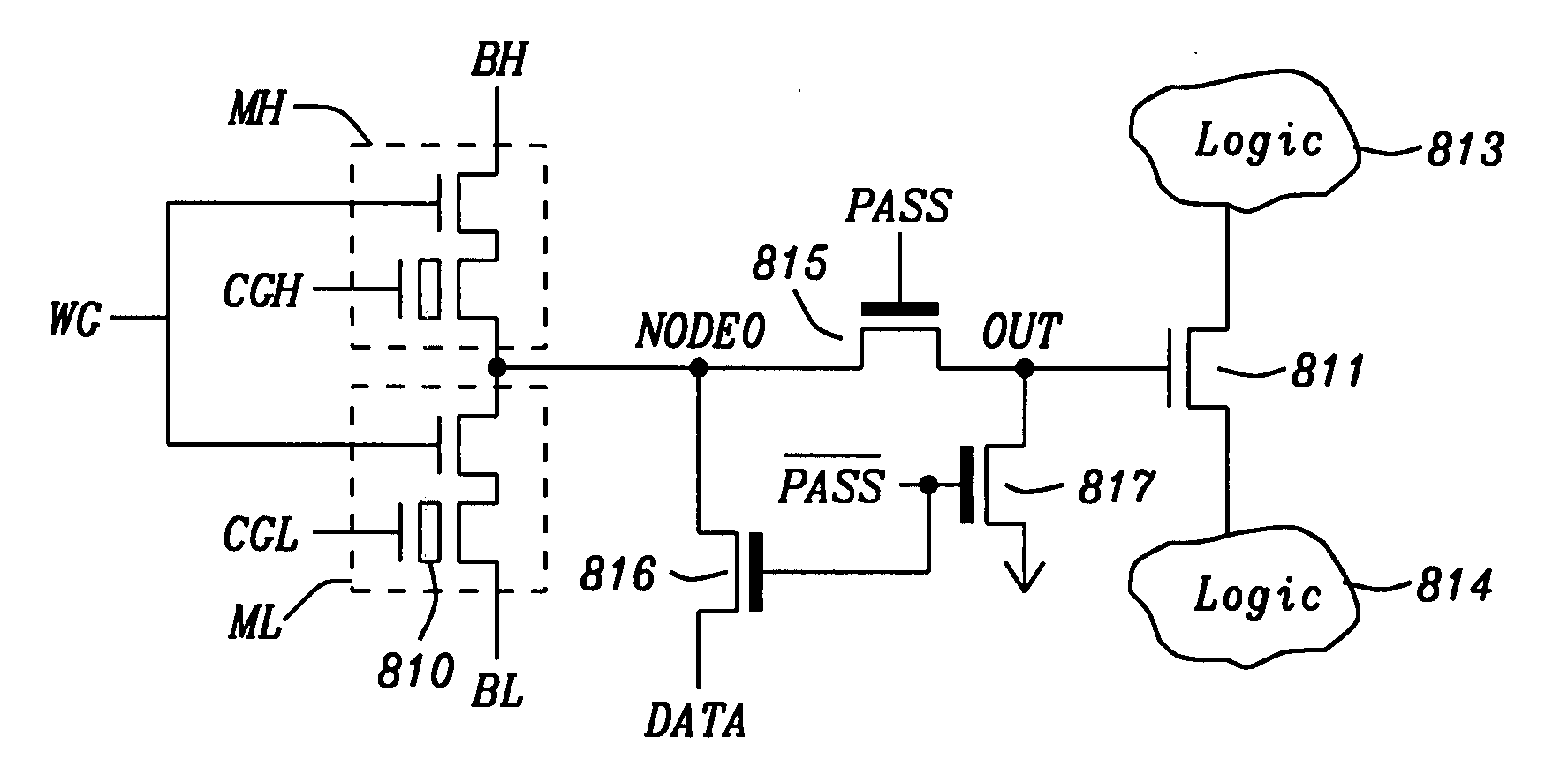
[0044]Continuing to refer to FIG. 10, the storage transistors MH and ML are decoupled from the logic interconnect transistor 711 during programming and erase operations by the pass transistor 715, the grounding transistor 717 and the data transistor 716. When the gate of the pass transistor 715 is high, the storage transistors MH and ML control the logic interconnect transistor. When the gate of the pass transistor is low, the gate of the logic interconnect transistor is grounded by the grounding transistor 717 to turn off the logic interconnect transistor 711 and protect the logic interconnect transistor from the high voltages of the erase and program operations of the two storage transistors MH and ML. The storage transistors MH and ML are programmed and erased in the present invention by tunneling electrons to and from the respective channel. TABLE 3 provides a tabulation of the approximate voltages required to program and erase the storage transistors MH and ML as well as read t...
fourth embodiment
[0045]In the present invention, the storage transistors MH and ML (circuit shown in FIG. 10) are programmed by channel hot electron tunneling and erased by hot hole injection, where the approximate voltages are shown in TABLE 4. As can be seen comparing tables 3 and 4 the program and erase voltages are different and the voltages in the PASS column in parenthesis are for the PASS BAR voltages needed to allow the higher DATA voltages to be connected to the storage transistors MH and ML.
PUM
 Abstract
Description
Claims
Application Information