Rectifier

a technology of rectifiers and rectifiers, applied in the field of rectifiers, can solve the problems of increasing the loss of devices in many applications, and achieve the effect of lowering the rise voltag

Inactive Publication Date: 2008-05-08
SHARP KK
View PDF3 Cites 20 Cited by
  • Summary
  • Abstract
  • Description
  • Claims
  • Application Information

AI Technical Summary

Benefits of technology

[0031] According to the present embodiment, by making the barrier layer have a layer thickness of not greater than 100 Å, at least part of the semiconducting channel is depleted in a thermal equilibrium state by bringing the gate electrode close to the semiconducting channel. With this arrangement, rectification operation such that a current flows bet...

Problems solved by technology

However, the fact that the rise voltage of the diode is not lower than 1.5 V ca...

Method used


Image

  • Rectifier
  • Rectifier
  • Rectifier

Examples


first embodiment

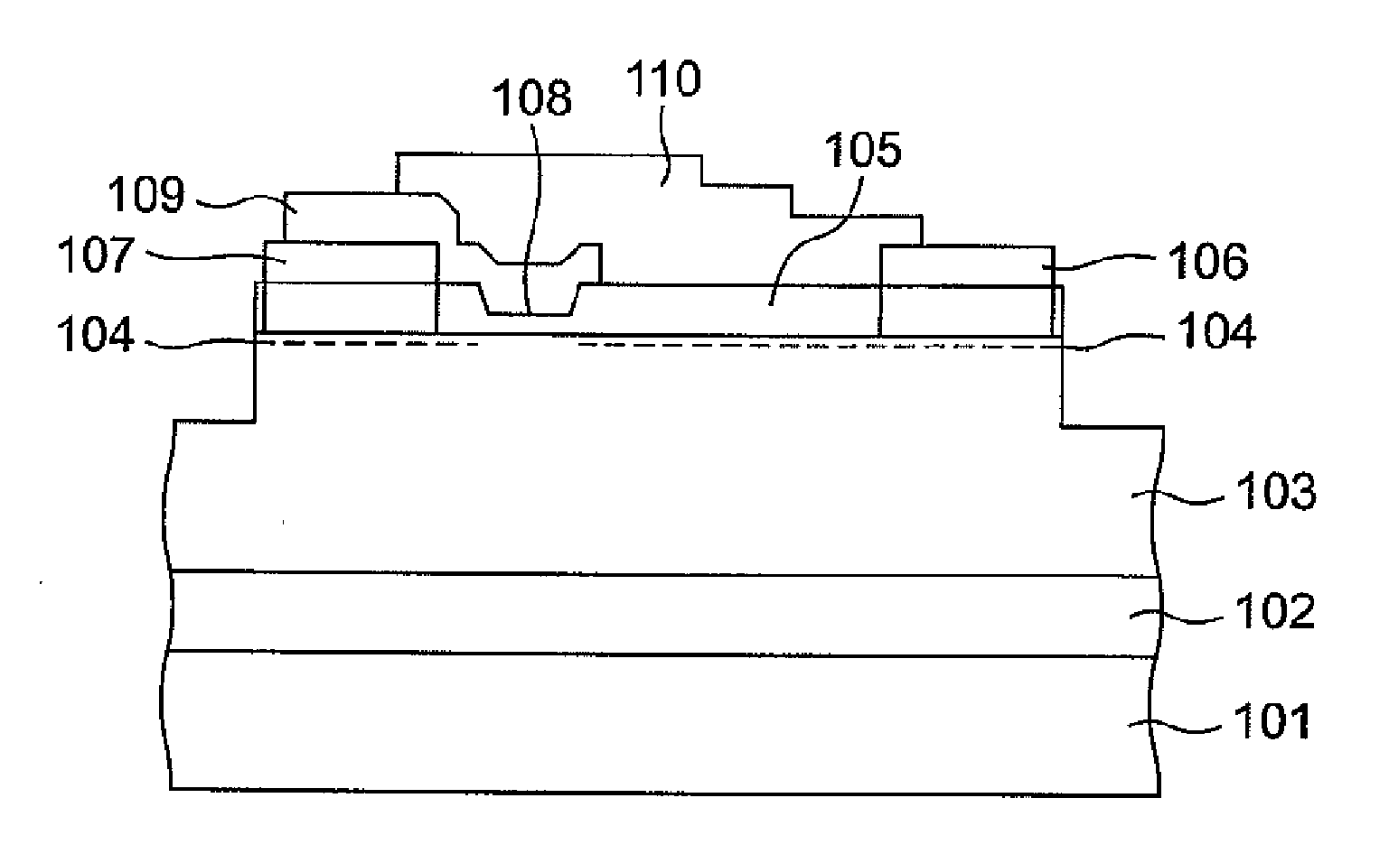
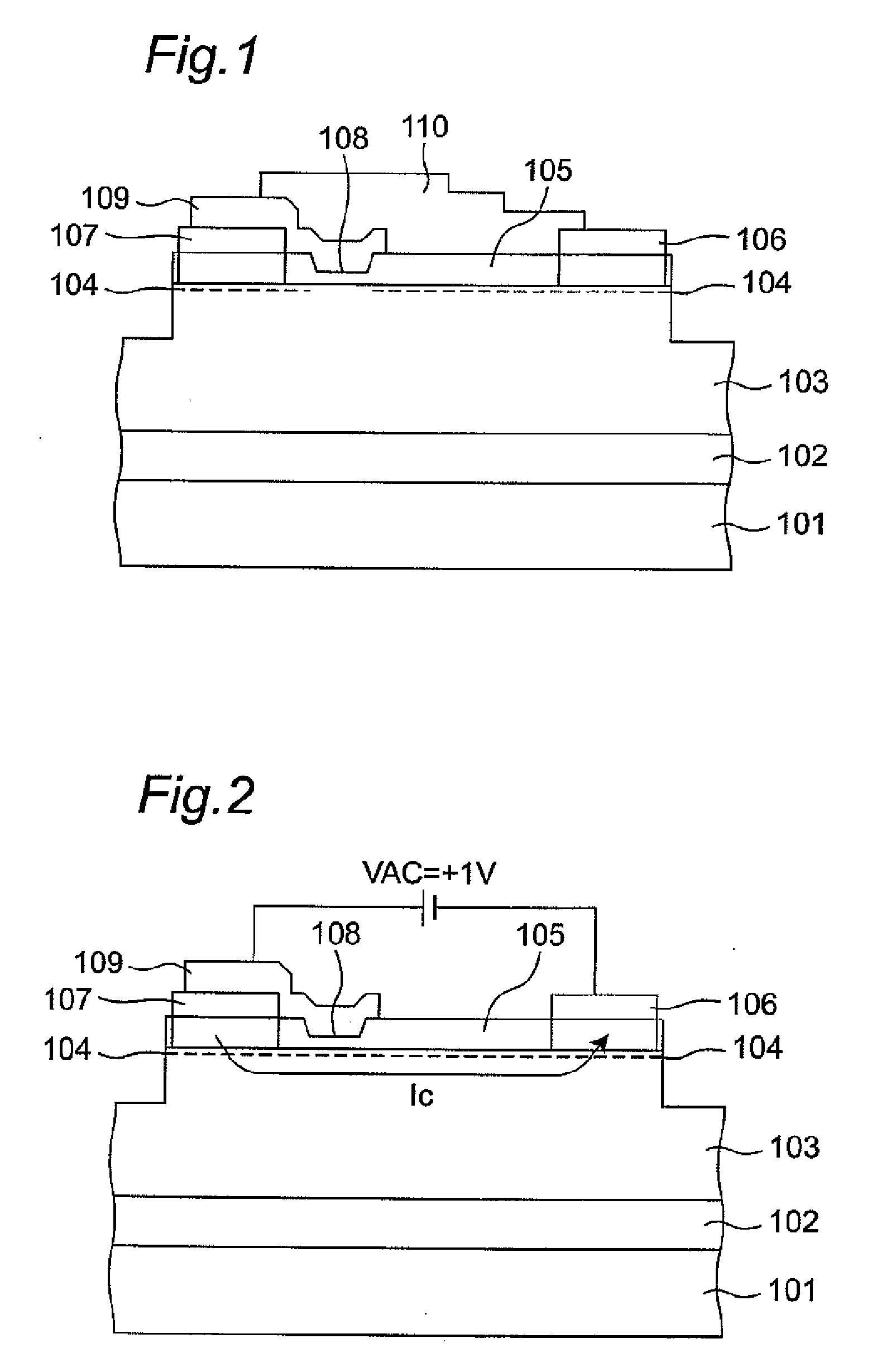
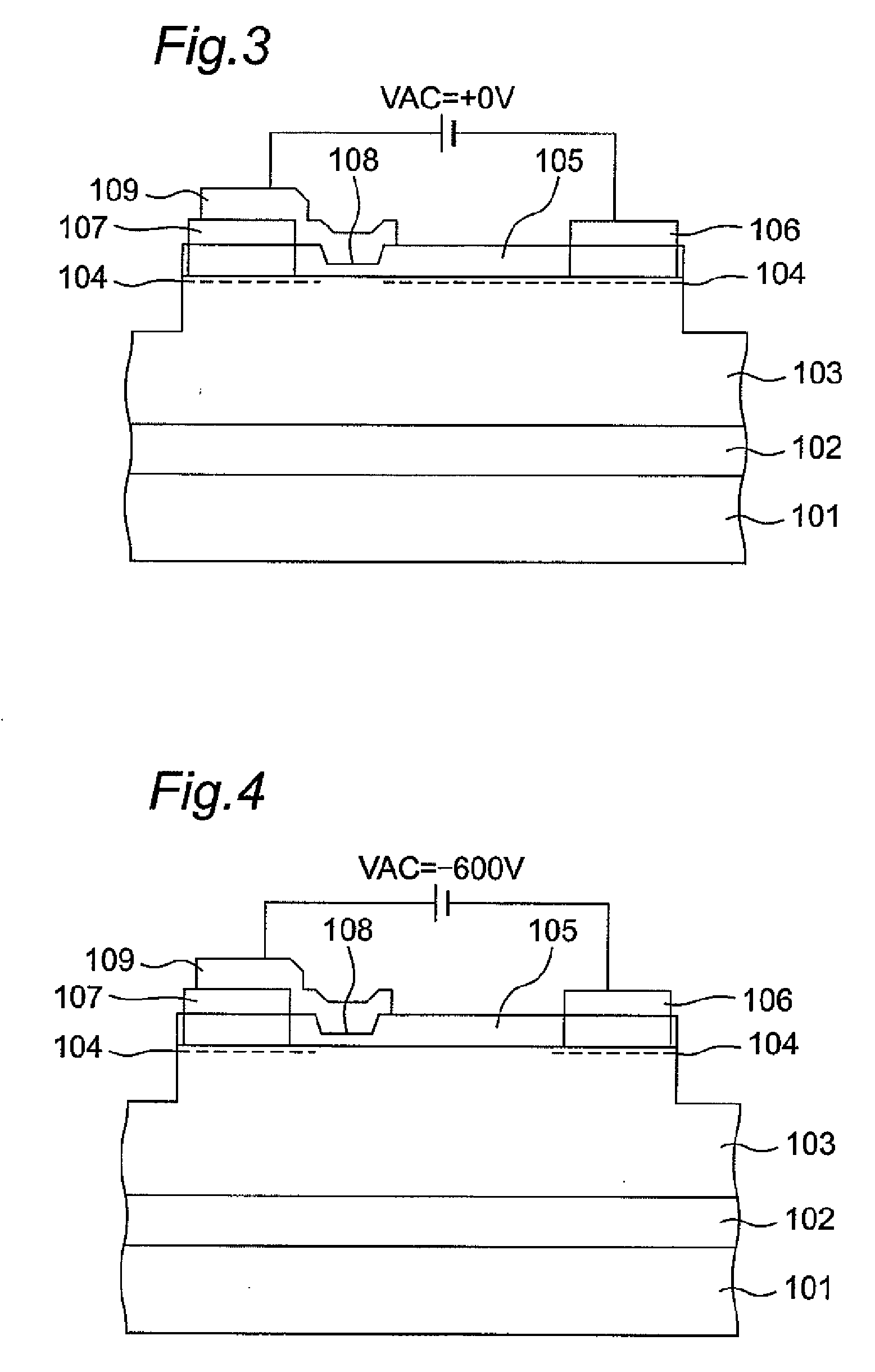
[0045]FIG. 1 shows the first embodiment of the rectifier of the present invention. In the rectifier, an AlN / GaN butter layer 102 having a layer thickness of 500 Å, a channel layer 103 made of undoped GaN having a layer thickness of 2 μm, and a barrier layer 105 made of Al0.3Ga0.7N having a layer thickness of 250 Å are successively formed on a silicon substrate 101.

[0046] An anode ohmic electrode 107 constructed of a laminate of Ti / Al / Au and a cathode ohmic electrode 106 constructed of a laminate of Ti / Al / Au are formed on the barrier layer 105. Then, a two-dimensional electron gas (2DEG) channel 104 is generated in the GaN channel layer 103 and in the vicinity of the boundary between the channel layer 103 and the AlGaN barrier layer 105.

[0047] The anode ohmic electrode 107 and the cathode ohmic electrode 106 are brought in ohmic contact with the two-dimensional electron gas channel 104 by heat treatment. Moreover, a recess 108 having a depth of 150 Å is formed by etching in the AlG...

second embodiment

[0055] Next, FIG. 5 shows the second embodiment of the rectifier of the present invention. In the second embodiment, an AlN / GaN buffer layer 502 having a layer thickness of 500 Å, a layer 511 made of undoped Al0.1Ga0.9N having a layer thickness of 2 μm, a channel layer 503 made of undoped GaN having a layer thickness of 500 Å, and a barrier layer 505 made of Al0.3Ga0.7N having a layer thickness of 250 Å are successively formed on a silicon substrate 501. The barrier layer 505, the channel layer 503 and the AlGaN layer 511 constitute a double heterojunction structure portion.

[0056] Moreover, a recess 508 having a depth of 150 Å is formed by etching in an AlGaN barrier layer 505. An anode ohmic electrode 507 constructed of a laminate of Ti / Al / Au is formed on the harrier layer 505 and within the recess 508. Moreover, a cathode ohmic electrode 506 constructed of a laminate of Ti / Al / Au is formed on the barrier layer 505. Then, a two-dimensional electron gas channel 504 is generated in t...

third embodiment

[0061] Next, FIG. 6 shows the third embodiment of the rectifier of the present invention. In the third embodiment, an AlN / GaN buffer layer 602 having a layer thickness of 500 Å, a channel layer 603 made of undoped GaN having a layer thickness of 2 μm, and a barrier layer 605 made of Al0.3Ga0.7N having a layer thickness of 250 Å are successively formed on a silicon substrate 601.

[0062] An anode ohmic electrode 607 constructed of a laminate of Ti / Al / Au and a cathode ohmic electrode 606 constructed of a laminate of Ti / Al / Au are formed on the barrier layer 605. Then, a two-dimensional electron gas (2DEG) channel 604 is generated in the GaN channel layer 603 and in the vicinity of the boundary between the channel layer 603 and the AlGaN barrier layer 605.

[0063] The anode ohmic electrode 607 and the cathode ohmic electrode 606 are brought in ohmic contact with the two-dimensional electron gas channel 604 by heat treatment. Moreover, a recess 608 having a depth of 180 Å is formed by etch...


PUM


Abstract

In the rectifier, a barrier layer and a channel layer constitute a heterojunction portion, and a two-dimensional electron gas channel is generated in the vicinity of a boundary between the channel layer and the barrier layer. A Schottky gate electrode is connected to an anode ohmic electrode and extends from above the anode ohmic electrode over to the barrier layer and a recess formed in the barrier layer is covered with the Schottky gate electrode. The two-dimensional electron gas channel located just below the recess is depleted by the influence of the Schottky gate electrode in a state in which there is no application voltage. By virtue of the formation of the recess in the barrier layer, the threshold voltage at which electrons are generated in the two-dimensional electron gas channel located just below the gate electrode is lowered, and the rise voltage can be made lower than that of the conventional Schottky diode.

Description

CROSS-REFERENCE TO RELATED APPLICATION [0001] This nonprovisional application claims priority under 35 U.S.C. §119(a) on Patent Application No(s). 2006-289626 filed in Japan on Oct. 25, 2006, the entire contents of which are hereby incorporated by reference. BACKGROUND OF THE INVENTION [0002] The present invention relates to a rectifier and for example, to a rectifier that has a heterojunction portion including a III-V group compound semiconductor of GaN or the like. [0003] Conventionally, for example, a GaN Schottky diode whose cross section is shown in FIG. 10 has been known as a rectifier (“Development of a GaN on Si electronic device for power supply” (Hirokazu Goto, Koji Ohtsuka), refer to The Institute of Electronics, Information and Communication Engineers, S45-S46, 2006). In the GaN Schottky diode, an AlN / GaN buffer layer 2002, a channel layer 2003 made of undoped GaN, and a layer 2005 made of Al0.25Ga0.75N are successively formed on an Si substrate 2001. A cathode ohmic ele...

Claims


Application Information

Patent Timeline
IPC IPC(8): H01L29/872
CPCH01L29/2003H01L29/861H01L29/7787
Inventor TWYNAM, JOHN
Owner SHARP KK
Why Eureka
Try Eureka