

Suspension board with circuit and producing method thereof
- Summary
- Abstract
- Description
- Claims
- Application Information
AI Technical Summary
Benefits of technology
Problems solved by technology
Method used
Image

Examples
example 1
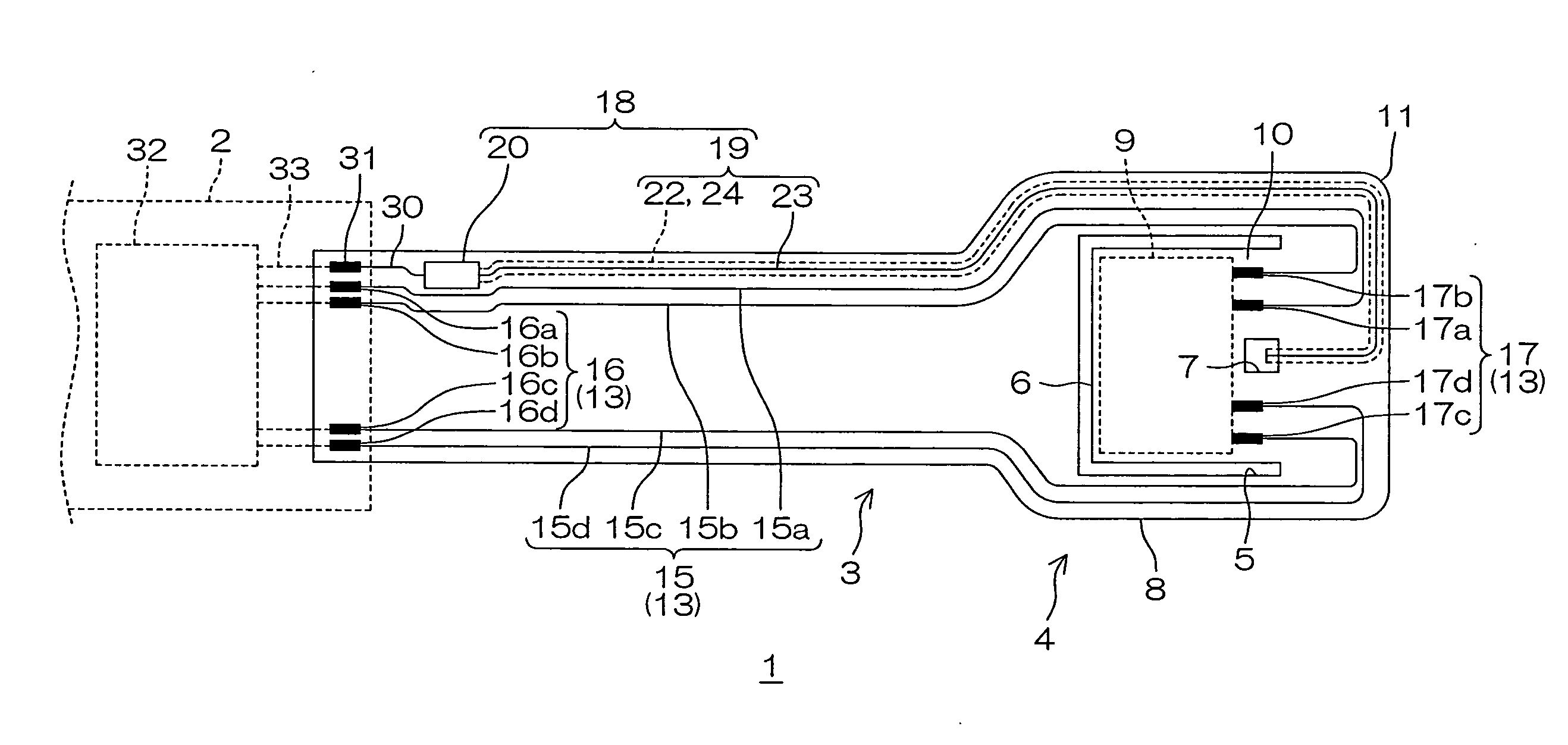
Embodiment in which Optical Waveguide is Provided on Insulating Base Layer
[0161]A metal supporting board made of a 20 μm thick stainless steel was prepared (cf. FIG. 4(a)).
[0162]Then, an insulating base layer of polyimide resin was formed on the metal supporting board in the above-mentioned pattern. The insulating base layer thus formed had a thickness of 10 μm.
[0163]Subsequently, a conductive pattern, and a supply wire and a supply terminal portion, all made of copper, were simultaneously formed by an additive method. These had a thickness of 10 μm.
[0164]Then, an insulating cover layer of polyimide resin was formed on the insulating base layer in the above-mentioned pattern. The insulating cover layer had a thickness of 5 μm. Thus, the insulating base layer, the conductive pattern, and the insulating cover layer were sequentially laminated on the metal supporting board (cf. FIG. 4(b)).
[0165]Next, an optical waveguide was formed on the insulating base layer. To form the optical wave...
example 2
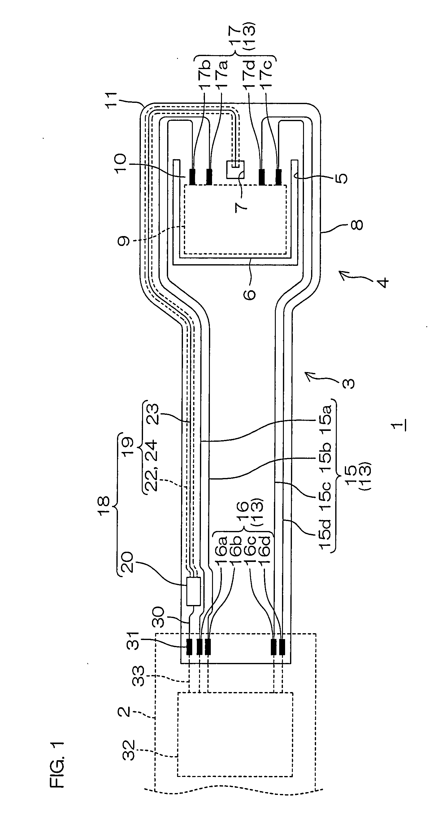
Embodiment in which Optical Waveguide is Provided on Insulating Cover Layer
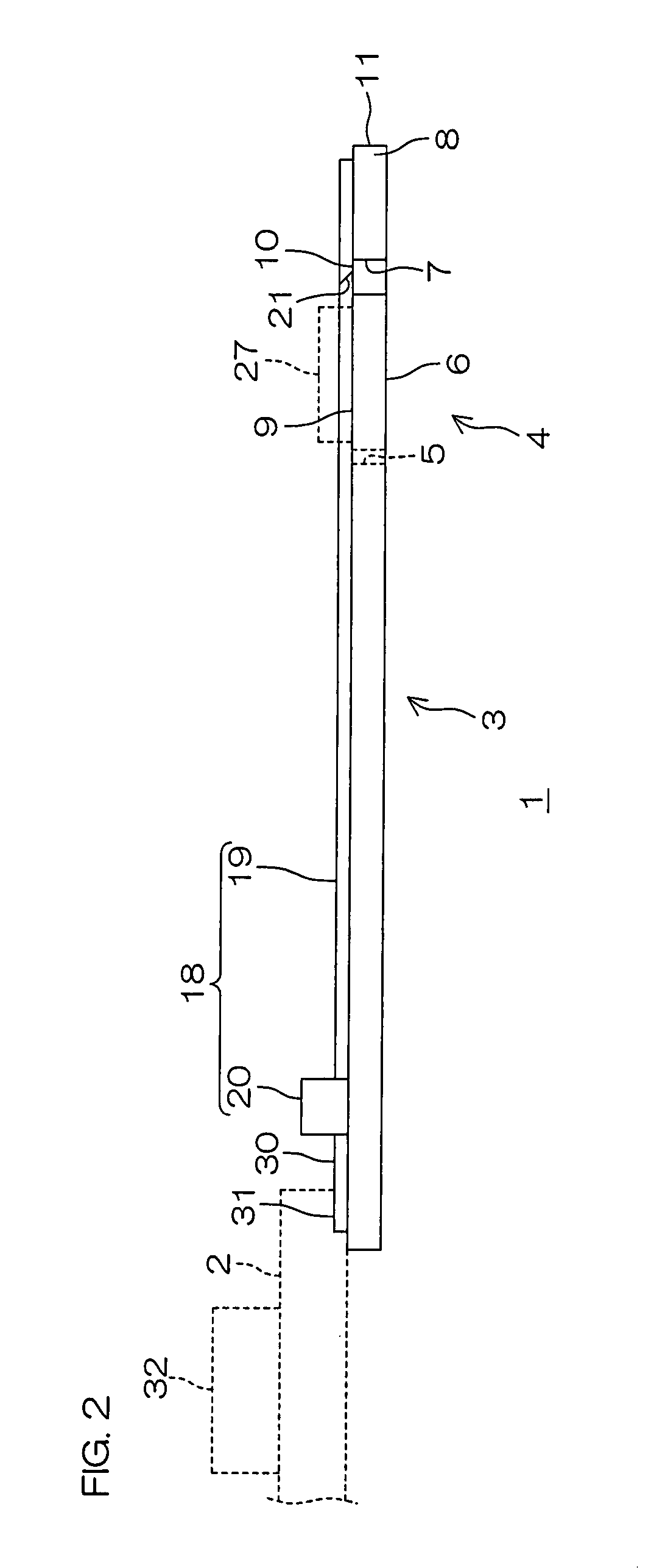
[0178]The suspension board with circuit was produced in the same method as in Example 1 except that the optical waveguide was provided on the insulating cover layer and the light emitting device was disposed on the insulating cover layer in Example 1 (cf FIGS. 1, 2, and 7).
[0179]That is, the insulating cover layer was formed so that the peripheral end edge thereof was in generally the same position in plane view as that of the insulating base layer (cf. FIG. 7(b)).
[0180]Further, the optical waveguide was formed on the insulating cover layer so as to be overlapped with the first wire in the wire portion and the outrigger portion of the gimbal portion, and be offset to the first wire portion and the other side in the widthwise direction in the terminal forming portion. Then, the light emitting device was disposed on the insulating cover layer.
example 3
Embodiment in which Insulating Base Layer, and Insulating Cover Layer also Serve as Over Clad Layer
[0181]A metal supporting board made of a 20 μm thick stainless steel was prepared (cf. FIG. 8(a)).
[0182]Then, an insulating base layer of polyimide resin was formed on the metal supporting board in the above-mentioned pattern. The insulating base layer had a refractive index of 1.541 at a wavelength of 830 nm, and had a thickness of 6 μm (cf. FIG. 8(b)).
[0183]Subsequently, a conductive pattern, and a supply wire and a supply terminal portion, all made of copper, are simultaneously formed on the insulating base layer by an additive method (cf. FIG. 8(c)). These had a thickness of 10 μm.
[0184]Then, a core layer was formed on the insulating base layer.
[0185]To form the core layer in the above-mentioned pattern, first, 70 parts by weight of bisphenoxyethanolfluorene diglycidyl ether (fluorene derivative, epoxy equivalent: 300 g / eq.), 30 parts by weight of 1,3,3-tris{4-[2-(3-oxetanyl)] buto...
PUM
| Property | Measurement | Unit |
|---|---|---|
| Thickness | aaaaa | aaaaa |
| Electrical conductor | aaaaa | aaaaa |
| Refractive index | aaaaa | aaaaa |
Abstract
Description
Claims
Application Information