Light Emitting Device Including Luminescent Ceramic and Light-Scattering Material

Active Publication Date: 2008-05-22
LUMILEDS
View PDF15 Cites 88 Cited by
  • Summary
  • Abstract
  • Description
  • Claims
  • Application Information

AI Technical Summary

Benefits of technology

[0008]In accordance with embodiments of the invention, a ceramic body comprising a wavelength converting material is disposed in the path of light emitted by the light emitting region of a semiconductor structure comprising a light emitting region disposed between an n-type region and a p-type region. A layer of transparent material is also disposed in the path of light emitted by the light emitting region. The transparent material may connect the ceramic body to the

Problems solved by technology

Many of these phosphor layers are fragile and difficult to handle, and are intolerant of the high temperature and high flux en

Method used


Image

  • Light Emitting Device Including Luminescent Ceramic and Light-Scattering Material
  • Light Emitting Device Including Luminescent Ceramic and Light-Scattering Material
  • Light Emitting Device Including Luminescent Ceramic and Light-Scattering Material

Examples


Example

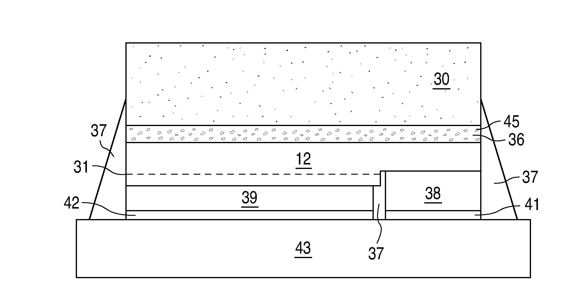
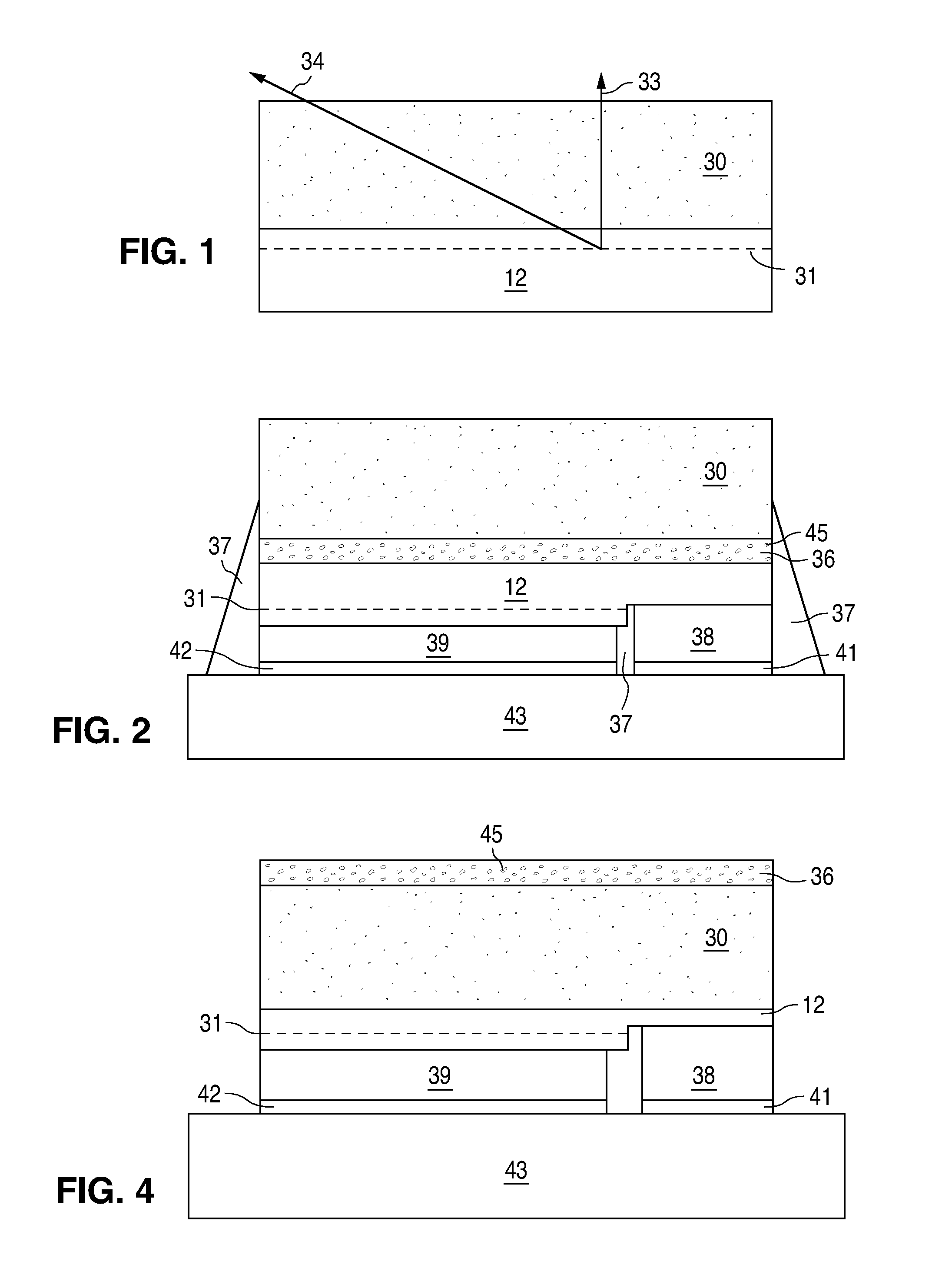
[0013]Luminescent ceramic layers may be made by heating a conventional powder phosphor under pressure until the surface of the phosphor particles begin to soften and melt. The partially melted particles stick together to form a rigid agglomerate of particles. Unlike a thin film, which optically behaves as a single, large phosphor particle with no optical discontinuities, a luminescent ceramic behaves as tightly packed individual phosphor particles, such that there are small optical discontinuities at the interface between different phosphor particles. Since the powder phosphor starting material is generally of uniform composition and doping, the resulting luminescent ceramic is generally transparent, optically homogenous, and uniformly doped throughout the ceramic slab with activating dopants that act as luminescent centers.

[0014]One problem with uniformly doped luminescent ceramics is the minimum thickness of the luminescent ceramic is limited by the ability to reproducibly manufac...


PUM

PropertyMeasurementUnit
Fractionaaaaaaaaaa
Thicknessaaaaaaaaaa
Thicknessaaaaaaaaaa

Abstract

A ceramic body comprising a wavelength converting material is disposed in the path of light emitted by the light emitting region of a semiconductor structure comprising a light emitting region disposed between an n-type region and a p-type region. A layer of transparent material is also disposed in the path of light emitted by the light emitting region. The transparent material may connect the ceramic body to the semiconductor structure. Particles configured to scatter light emitted by the light emitting region are disposed in the layer of adhesive material. In some embodiments the particles are phosphor; in some embodiments the particles are not a wavelength-converting material.

Description

BACKGROUND[0001]1. Field of Invention[0002]The present invention relates to wavelength-converted semiconductor light emitting devices.[0003]2. Description of Related Art[0004]Semiconductor light-emitting devices including light emitting diodes (LEDs), resonant cavity light emitting diodes (RCLEDs), vertical cavity laser diodes (VCSELs), and edge emitting lasers are among the most efficient light sources currently available. Materials systems currently of interest in the manufacture of high-brightness light emitting devices capable of operation across the visible spectrum include Group III-V semiconductors, particularly binary, ternary, and quaternary alloys of gallium, aluminum, indium, and nitrogen, also referred to as III-nitride materials. Typically, III-nitride light emitting devices are fabricated by epitaxially growing a stack of semiconductor layers of different compositions and dopant concentrations on a sapphire, silicon carbide, III-nitride, or other suitable substrate by ...

Claims


Application Information

Patent Timeline
IPC IPC(8): H01L33/00H01L33/44H01L33/50
CPCC04B35/584C04B2235/3213C04B2235/3215C04B2235/3224C04B2235/3865C04B2235/3873H05B33/14C09K11/7734C09K11/7774H01L33/44H01L33/501H01L2933/0091C09K11/7731C09K11/77348
Inventor MUELLER, GERD O.MUELLER-MACH, REGINA B.
Owner LUMILEDS
Why Eureka
Try Eureka