Method and system for lithography simulation and measurement of critical dimensions

a lithography simulation and critical dimension technology, applied in the field of lithograph technology, can solve the problems of image quality degradation and resolution limits, differences between intended patterns and images obtained by lithography technology, and serious degradation of image quality, so as to improve the quality and accuracy of lithography technology, the effect of small computing time and efficient quality control

Inactive Publication Date: 2008-05-22
CADENCE DESIGN SYST INC
View PDF10 Cites 10 Cited by
  • Summary
  • Abstract
  • Description
  • Claims
  • Application Information

AI Technical Summary

Benefits of technology

[0012]Computer simulation is an efficient means to investigate differences between intended patterns and obtained images. CD (Critical Dimension) measurements that measure critical dimensions of the image based on the computer simulation results are important and helpful. CD measurement results in conjunction with quality control of semiconductor manufacturing process can contribute yield improvement and efficient quality control.
[0013]To achieve the above mentioned objectives, the concepts listed below contribute to improvement of quality and accuracy of lithography technology: (1) a method and equipment for fast lithography simulation and CD measurement

Problems solved by technology

A fundamental problem with conventional lithograph technologies is image quality degradation and resolution limits caused by chemical and physical effects in the process of the technologies.
An example of such phenomena is proximity effect, which occurs in both electron beam writing and optical projection lithography and causes differences between intended patterns and images obtained by the lithography technologies.
This degradation of the image quality becomes serious when the image is finer.
This simulation method still has a problem, wherein these simulators consume huge amounts of computing time for obtaining the lithography image for large area similar to a whole LSI chip.
Specifying the CD measurement points is also tedious and time consuming work when the objective area becomes large.
Even if CD measurement results are ob

Method used


Image

  • Method and system for lithography simulation and measurement of critical dimensions
  • Method and system for lithography simulation and measurement of critical dimensions
  • Method and system for lithography simulation and measurement of critical dimensions

Examples


Embodiment Construction

[0038]Various embodiments of the present invention are described hereinafter with reference to the drawings. It should be noted that the drawings are not drawn to scale and that elements of similar structures or functions are represented by like reference numerals throughout the drawings.

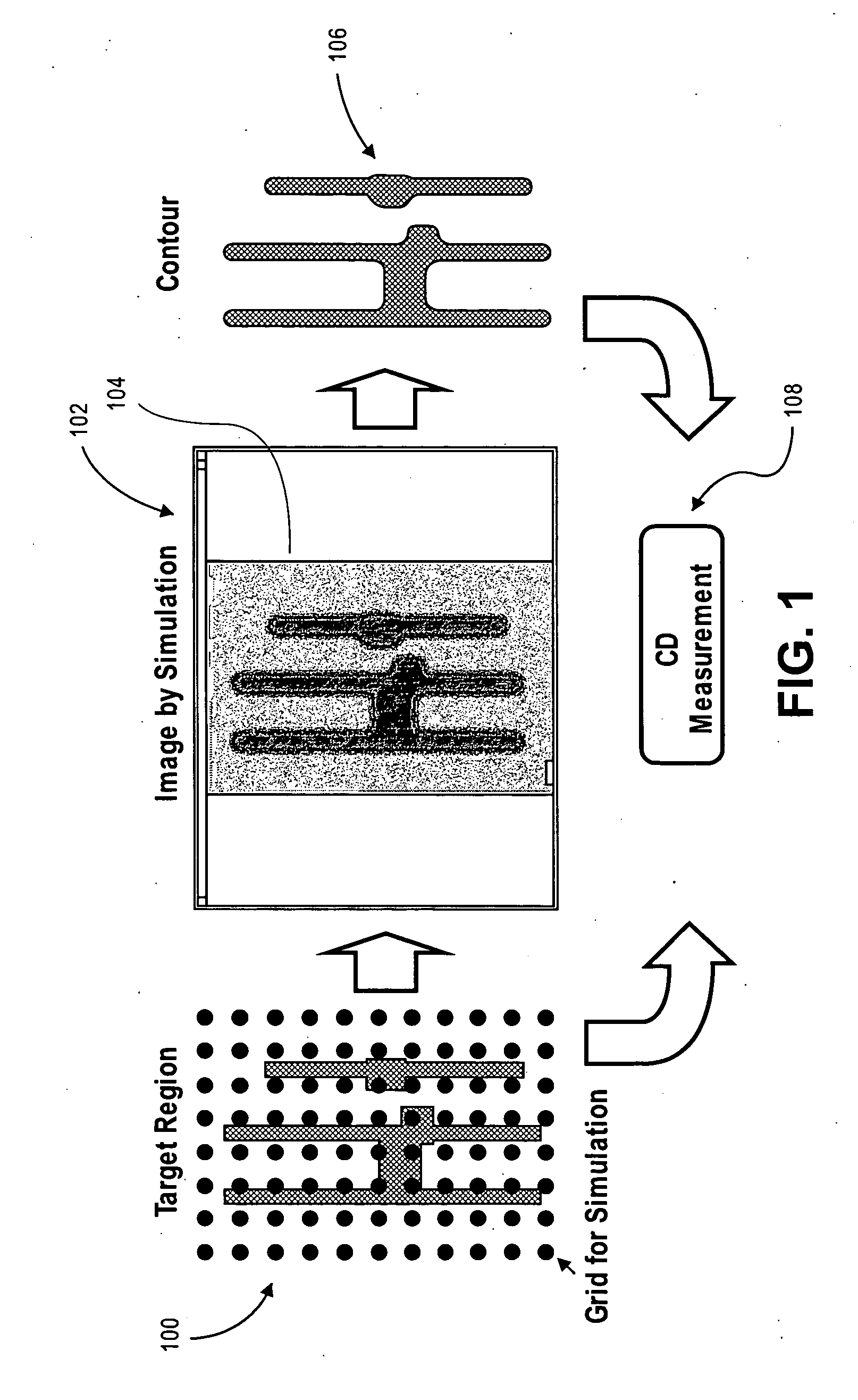
[0039]FIG. 1 shows conventional lithography simulation and procedure of CD measurement by the simulation. A target region 100 is an area where lithography simulation is performed. A grid 102 for simulation is a set of points that covers the target region100 and intensity of the lithography is calculated at the points. An image 104 of the lithography obtained by the simulation, and contour 106 of the intensity.

[0040]Lithography is an indispensable technology for modern fine manufacturing. In the semiconductor industry, for example, it is relatively difficult to build a semiconductor manufacture process without lithography technologies. Other examples include fabrication of MEMS (Micro Electro-Mechani...


PUM


Abstract

A method and system for lithography simulation is disclosed. The method and system specify a subject region of a lithography image with a CD marker, specify a threshold intensity over the lithography image, specify a gradient to a threshold value of the threshold intensity, and calculate a sensitivity or ratio of change of an image boundary of the lithography image to lithography process variation.

Description

BACKGROUND[0001]1. Field[0002]The field of the present invention relates to lithograph technology for fine image fabrication, and in particular to a lithography simulation system and measurement of critical dimensions.[0003]2. Description of Related Art[0004]Fine image fabrication by lithography uses technologies like particle beam writers for writing fine images on a plate coated by a particle beam sensitive resist and an optical projection lithography method that uses a mask having transparent and opaque parts on the surface of the mask for generating a fine image on a plate coated by a photo sensitive resist. An example of particle beam writers is an electron beam writer that is used for writing fine images on both silicon wafers and masks for optical projection lithography. A technology that uses electron beam writers for making fine images for semiconductor integrated circuits directly on the semiconductor wafer is called Electron Beam Direct Writing (EBDW) technology. EBDW tec...

Claims


Application Information

Patent Timeline
IPC IPC(8): G06G7/48
CPCG03F1/144G03F7/2061G03F1/36G03F1/68
Inventor HARA, DAISUKEMITSUHASHI, TAKASHIWU, ZHIGANG
Owner CADENCE DESIGN SYST INC
Why Eureka
Try Eureka