Composite light-emitting material and light-emitting device comprising the same

a technology of light-emitting devices and composite light-emitting materials, which is applied in the field of composite light-emitting materials and light-emitting devices comprising the same, can solve the problems of lowering the luminous efficiency of semiconductor nanocrystals, prone to surface defects, and affecting the operation of light-emitting devices, so as to achieve efficient regulation of the characteristics of light-emitting devices and simplify the application procedure

Active Publication Date: 2008-05-29
SAMSUNG ELECTRONICS CO LTD
View PDF6 Cites 62 Cited by
  • Summary
  • Abstract
  • Description
  • Claims
  • Application Information

AI Technical Summary

Benefits of technology

[0013]Therefore, the present invention has been made in view of the above-described problems, and one aspect of the present invention includes providing a composite light-emitting material which is capable of simplifying the procedure

Problems solved by technology

Since the semiconductor nanocrystal has a relatively large surface area due to its very small size, it is apt to raise any defects on the surface thereof.
These defects function as various energy traps in the band gap energy, thereby lowering the luminous efficiency of the semiconductor nanocrystal.
Moreover, this phenomenon becomes more serious if semiconductor nanocrystals are combined.
Further, when electrons continuously accumulate on the surface, it is hard to get them to an excitation state owing to the charging thereof, which may lead to the reduction in the luminous efficiency.
Meanwhile, in the case of the organic dye used as a light-emitting mate

Method used


Image

  • Composite light-emitting material and light-emitting device comprising the same
  • Composite light-emitting material and light-emitting device comprising the same
  • Composite light-emitting material and light-emitting device comprising the same

Examples


preparation example 1

Preparation of Semiconductor Nanocrystals

[0074]About 32 grams (g) of trioctylamine (hereinafter, referred to as “TOA”), about 1.8 g of oleic acid and about 1.6 millimoles (mmol) of cadmium oxide were simultaneously added to a 125 milliliter (ml) flask equipped with a reflux condenser and stirred at a controlled reaction temperature of about 300 degrees Celsius (°C.). About 2 ml of a 2 molar (M) Se-TOP (trioctylphosphate) complex solution was rapidly added to the reaction mixture, and about 90 seconds after the addition, about 0.08 mmol of an octylthiol complex solution mixed with about 6 mlof TOA was gradually poured thereto. After the reaction for about 40 minutes, about 16 ml of a zinc oleate complex solution that was separately prepared was gradually added to the resulting reaction mixture.

[0075]The zinc oleate complex solution was prepared by adding about 4 mmol of zinc acetate, about 2.8 g of oleic acid and about 16 g of TOA to a 125 ml flask equipped with a reflux condenser an...

example 1

Preparation of a Composite Light-Emitting Material

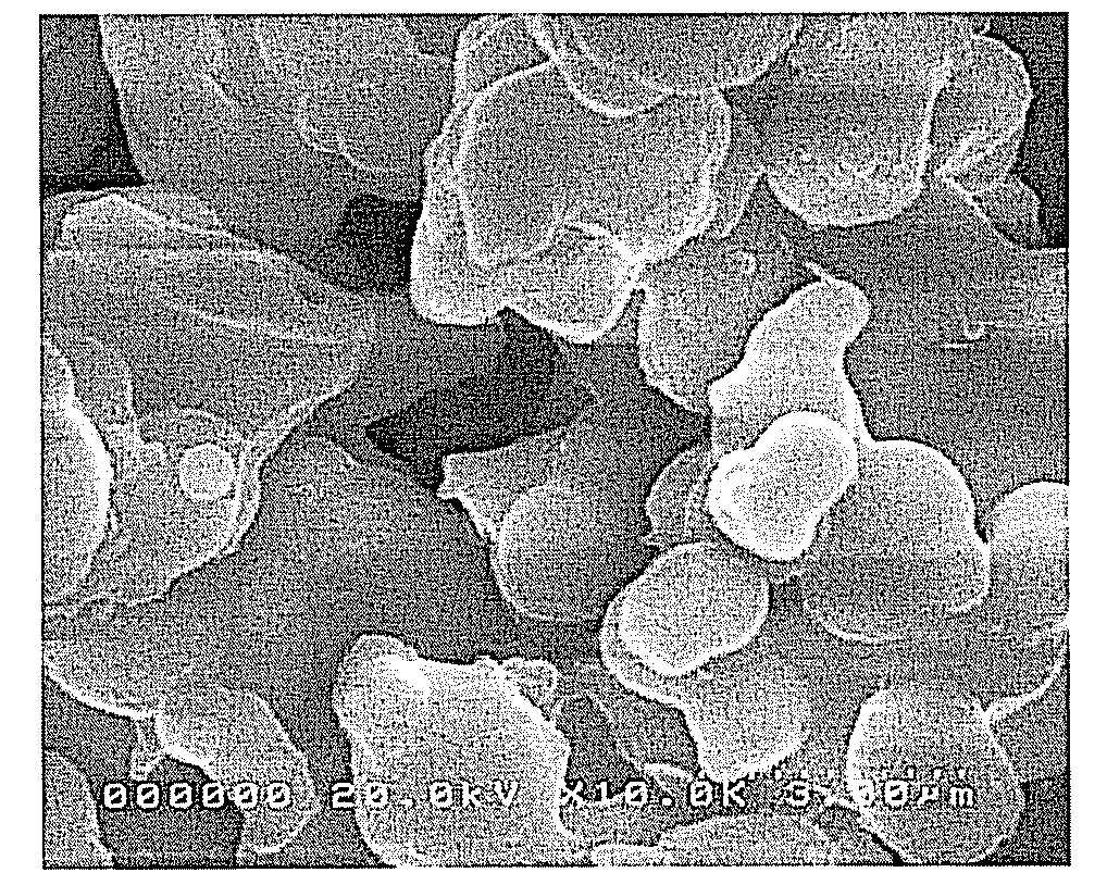
[0078]After about 100 milligrams (mg) of the red light-emitting semiconductor nanocrystal prepared in Preparation Example 1 was separated by centrifugation, about 205 mg of 5-amino-1-pentanol being present in the amount of about 50 percent (%) by weight in ethanol was added thereto, and the mixture was stirred at room temperature for about 30 minutes so as to be evenly dispersed. About 300 mg of ethanol was added to the stirred mixture and further stirred again at room temperature for about 30 minutes, to obtain a solution in which the semiconductor nanocrystals are dispersed homogeneously. About 10 mg of triethoxysilylpropyl isocyanate was again added to the solution followed by adding about 50 mg of 3-aminopropyltrimethoxysilane thereto. The resulting mixture was stirred at room temperature for about 5 minutes, mixed with about 0.2 g of a green light-emitting phosphor TG-3540 (manufactured by Sarnoff Corporation), and then further ...

example 2

Preparation of a Composite Light-Emitting Material

[0080]After about 100 mg of the red light-emitting semiconductor nanocrystal prepared in Preparation Example 1 was separated by centrifugation, it was dispersed in chloroform as a solvent in the amount of about 1% by weight. Separately, about 0.05 g of polymethyl methacrylate (PMMA) having a weight average molecular weight of about 15,000 was dissolved in about 2.5 ml of chloroform and sufficiently stirred at room temperature for about an hour or more. About 0.3 ml of the semiconductor nanocrystal solution prepared above was added to the PMMA solution and stirred so as to form a homogeneous mixture. About 0.2 g of a green light-emitting phosphor TG-3540 (manufactured by Sarnoff Corporation) was added to the mixture and further stirred at room temperature for about 2 hours. The stirred solution was centrifuged as-is to separate a precipitate. The precipitate thus obtained was heated to about 50° C. so as to evaporate the solvent, to o...


PUM


Abstract

Disclosed herein are a composite light-emitting material, which includes two or more light-emitting materials selected from an inorganic phosphor, a semiconductor nanocrystal and an organic dye in which the surfaces of the two or more light-emitting materials are coated; and a light-emitting device comprising the same, so as to improve the luminous efficiency and lifetime.

Description

[0001]This non-provisional application claims priority to Korean Patent Application No. 10-2006-0078707 filed on Aug. 21, 2006, and all the benefits accruing therefrom under 35 U.S.C. §119, the contents of which are herein incorporated by reference in its entirety.BACKGROUND OF THE INVENTION[0002]1. Field of the Invention[0003]The present invention relates to a composite light-emitting material and a light-emitting device comprising the same. More particularly, the present invention relates to a composite light-emitting material comprising two or more light-emitting materials of an inorganic phosphor, a semiconductor nanocrystal and an organic dye in which the surfaces of the two or more light-emitting materials are coated, and a light-emitting device comprising the same.[0004]2. Description of the Related Art[0005]Light-emitting materials exhibiting emission properties caused by an energy stimulus have been widely used in display devices such as light source devices, cathode ray tu...

Claims


Application Information

Patent Timeline
IPC IPC(8): C09K11/06C09K11/54C09K11/08C09K11/77C09K11/88H01L33/44H01L33/50
CPCC09K11/025C09K11/565C09K11/881Y10T428/2949C09K11/89C09K11/892H01L33/502C09K11/883
Inventor JANG, EUN JOOJUN, SHIN AELIM, JUNG EUN
Owner SAMSUNG ELECTRONICS CO LTD
Why Eureka
Try Eureka