Semiconductor Devices Having Low Threading Dislocations and Improved Light Extraction and Methods of Making the Same

a technology of semiconductors and dislocations, applied in the field of semiconductor devices, can solve problems such as problems such as problems such as problems such as problems such as problems such as the disadvantage of electrical insulation of sapphire, the inability to manufacture leds using heteroepitaxial growth on substrates such as silicon carbide or sapphire, and achieve the effect of improving radiation extraction efficiency and reducing defects

Active Publication Date: 2008-05-29
CREELED INC
View PDF44 Cites 53 Cited by
  • Summary
  • Abstract
  • Description
  • Claims
  • Application Information

AI Technical Summary

Benefits of technology

[0012]The present invention further includes methods for fabricating a semiconductor device structure suitable for use in the fabrication of electronic devices such as LEDs. The method of the invention includes the step of treating a substrate growth surface suitable for supporting the growth of an epitaxial region thereon to roughen the growth surface. The substrate gro

Problems solved by technology

However, gallium nitride (GaN) presents a particular set of technical problems in manufacturing working devices.
The primary problem is the lack of bulk single crystals of gallium nitride which in turn means that gallium nitride or other Group III nitride devices must be formed as epitaxial layers on other materials.
Sapphire offers the disadvantage, however, of being an electrical insulator.
This means that the electric current that is passed through an LED to generate the emission cannot be directed through the sapphire substrate.
Despite the advantages of these and other LED devices, the fabrication of LEDs using heteroepitaxial growth on substrates such as silicon carbide or sapphire can be problematic.
Such mismatches, and the strain they produce, can carry with them the potential for crystal defects, which in tu

Method used


Image

  • Semiconductor Devices Having Low Threading Dislocations and Improved Light Extraction and Methods of Making the Same
  • Semiconductor Devices Having Low Threading Dislocations and Improved Light Extraction and Methods of Making the Same
  • Semiconductor Devices Having Low Threading Dislocations and Improved Light Extraction and Methods of Making the Same

Examples


Embodiment Construction

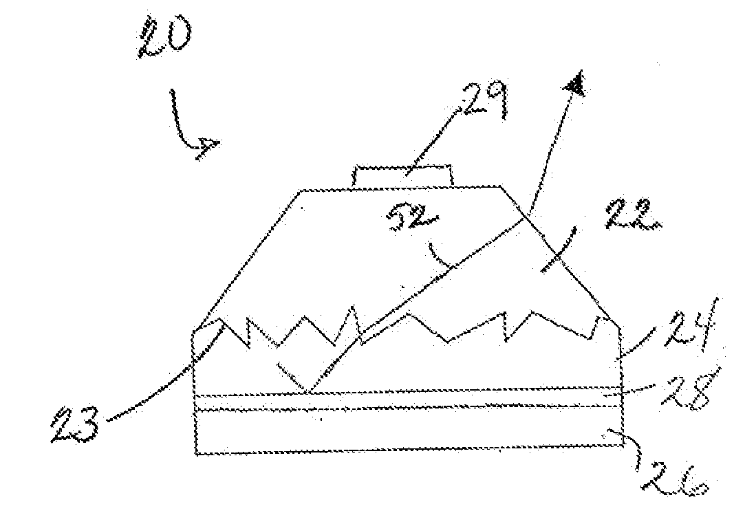
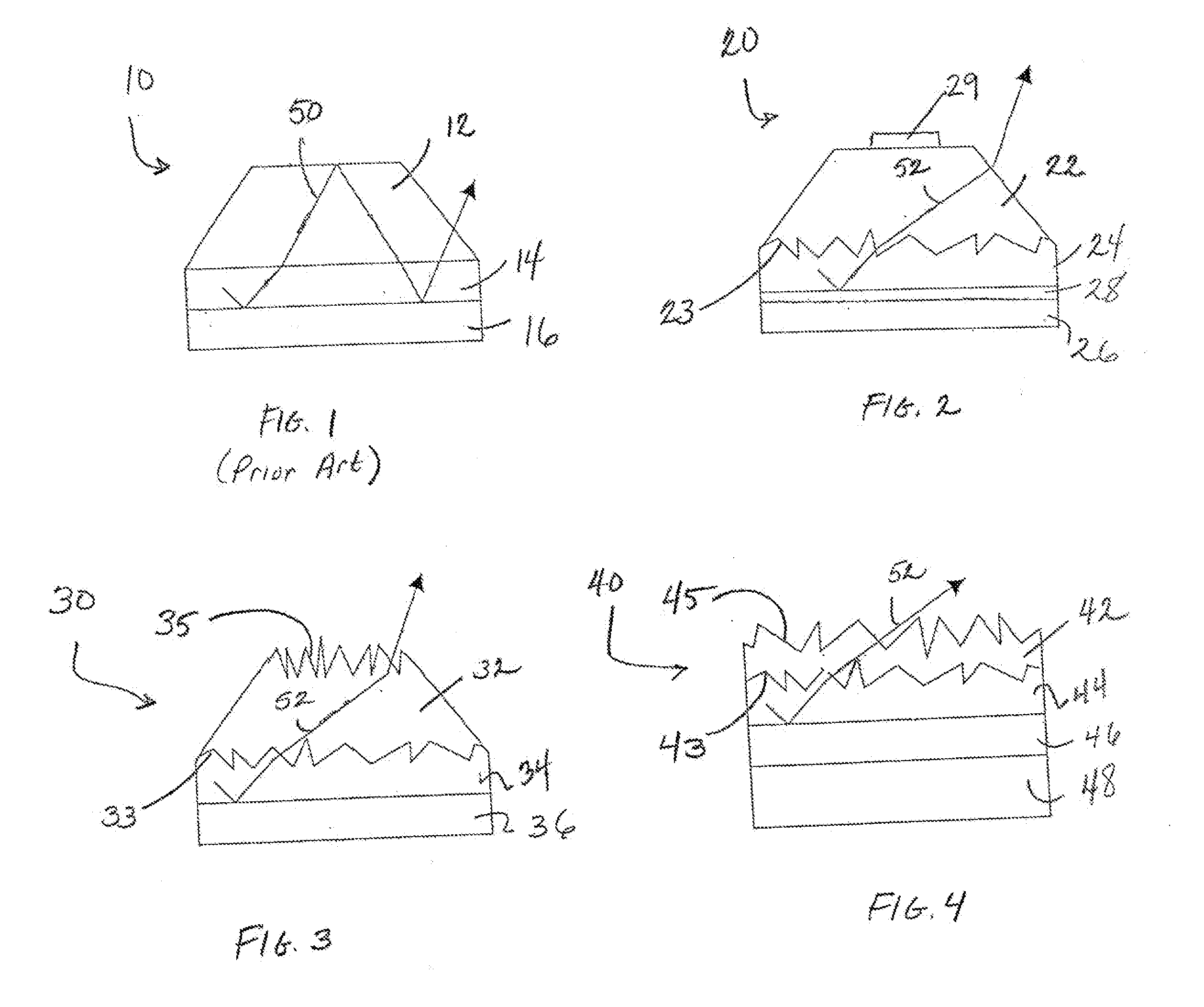
[0025]The present invention now will be described more fully hereinafter with reference to the accompanying drawings, in which some, but not all embodiments of the invention are shown. Indeed, this invention may be embodied in many different forms and should not be construed as limited to the embodiments set forth herein; rather, these embodiments are provided so that this disclosure will satisfy applicable legal requirements. Like numbers refer to like elements throughout the specification.

[0026]The terminology used herein is for the purpose of describing particular embodiments only and is not intended to be limiting of the invention. As used herein the term “and / or” includes any and all combinations of one or more of the associated listed items. As used herein, the singular forms “a,”“an” and “the” are intended to include the plural forms as well, unless the context clearly indicates otherwise. It will be further understood that the terms “comprises” and / or “comprising,” when used...


PUM


Abstract

Semiconductor device structures are provided that are suitable for use in the fabrication of electronic devices such as light emitting diodes. The semiconductor device structures include a substrate having a roughened growth surface suitable for supporting the growth of an epitaxial region thereon. The device structure can include an epitaxial region having reduced defects and/or improved radiation extraction efficiency on the roughened growth surface of the substrate. The roughened growth surface of the substrate can have an average roughness Ra of at least about 1 nanometer (nm) and an average peak to valley height Rz of at least about 10 nanometers (nm).

Description

BACKGROUND OF THE INVENTION[0001]The present invention relates to semiconductor devices and, more particularly, to semiconductor devices useful in the fabrication of light emitting diodes (LEDs).[0002]Light emitting diodes (LEDs) are an important class of solid-state devices that convert electric energy to light. LEDs generally include an active layer of semiconductor material sandwiched between two oppositely doped layers. When a bias is applied across the doped layers, holes and electrons are injected into the active layer where they recombine to generate light. Light is emitted omnidirectionally from the active layer and from all surfaces of the LED. Recent advances in LEDs (such as nitride based LEDs) have resulted in highly efficient light sources that surpass the efficiency of filament-based light sources, providing light with equal or greater brightness in relation to input power.[0003]Successful materials for producing LEDs (including light emitting diodes, laser diodes, pho...

Claims


Application Information

Patent Timeline
IPC IPC(8): H01L33/00H01L21/20H01L29/06
CPCH01L21/02378H01L21/02392H01L21/02395H01L21/02403H01L21/0242Y02E10/50H01L21/0254H01L21/02658H01L31/0236H01L33/007H01L21/02425H01L31/02363
Inventor BERGMANN, MICHAEL JOHNHANSEN, JASONEMERSON, DAVID TODDHABERERN, KEVIN WARD
Owner CREELED INC
Why Eureka
Try Eureka