Flip-Chip Light Emitting Diodes and Method of Manufacturing Thereof

a light-emitting diode and flip-chip technology, which is applied in the manufacture of semiconductor/solid-state devices, semiconductor devices, electrical devices, etc., can solve the problems of low light-utilization efficiency, reduced device life, and difficulty in high-brightness light-emitting devices, so as to improve luminous efficiency and life span, improve ohmic contact properties, and increase the efficiency of wire bonding and yield

Active Publication Date: 2008-05-29
SAMSUNG ELECTRONICS CO LTD
View PDF8 Cites 17 Cited by
  • Summary
  • Abstract
  • Description
  • Claims
  • Application Information

AI Technical Summary

Benefits of technology

[0040]As described hereinbefore, in accordance with a flip-chip nitride-based light emitting device of the present invention and a process for preparing the same, there are provided advantages such as improved ohmic contact properties with the p-type clad layer, leading to increased wire bonding efficiency and yield upon packaging the light emitting device, capability to improve luminous efficiency and life span of the device due to low specific contact resistance and excellent current-voltage properties.

Problems solved by technology

However, top-emitting light emitting diodes utilizing semi-transparent electrode thin films made up of nickel / gold have low light-utilization efficiency, thus making it difficult to realize high-capacity, high-brightness light emitting devices.
Meanwhile, such metal materials for reflective layers have high reflection efficiency and therefore can provide high transient luminous efficiency, but suffer from difficulty to form ohmic contacts having low resistance values due to low work function thereof, resulting in reduced life span of the device and poor adhesion to gallium nitride thus failing to provide stable device reliability.
Firstly, aluminum (Al) exhibits a low work function and easily forms nitrides (AlN) even at relatively low annealing temperatures, thus making it difficult to form ohmic contact with the p-type gallium nitride.
Next, silver (Ag) forms high quality ohmic contact and exhibits high reflectivity, but is heat-labile, thus suffering form difficulty to form high quality thin films via thin film forming processes.
That is, silver (Ag) thin films exhibit agglomeration at the early stages of annealing due to heat-lability thereof and undergo changes into voids, hillocks and islands at the final stages of annealing, thus resulting in degradation of electrical and optical properties.
2066), but these structures suffer from difficulty to form ohmic contacts and therefore raise problems associated with generation of large quantities of heat due to a high operation voltage upon operation of light emitting diodes.
However, these electrode structures also have shortcomings such as low adhesion and reduced luminous efficiency due to reflective scattering.

Method used


Image

  • Flip-Chip Light Emitting Diodes and Method of Manufacturing Thereof
  • Flip-Chip Light Emitting Diodes and Method of Manufacturing Thereof
  • Flip-Chip Light Emitting Diodes and Method of Manufacturing Thereof

Examples


first embodiment

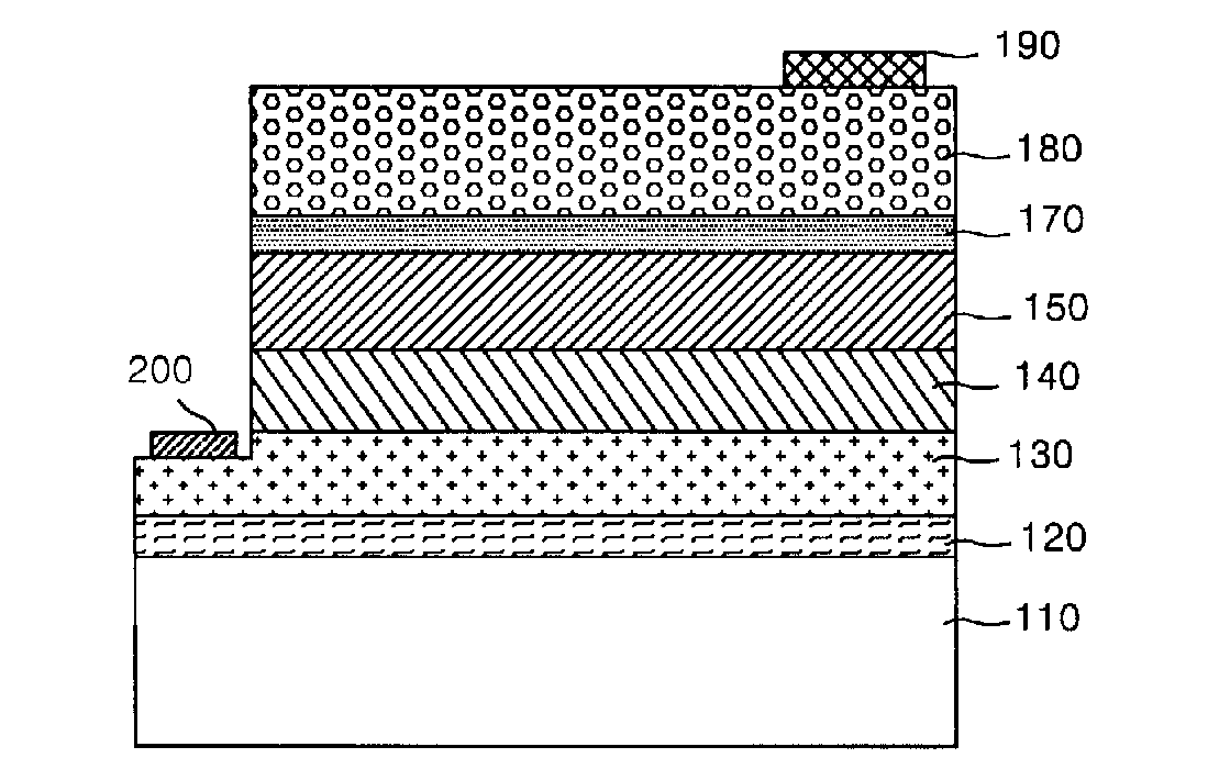
[0050]FIG. 1 shows a cross-sectional view of a flip-chip nitride-based light emitting device in accordance with the present invention.

[0051]Referring now to FIG. 1, the flip-chip nitride-based light emitting device is formed of a structure including a substrate 110, a buffer layer 120, an n-type clad layer 130, an active layer 140, a p-type clad layer 150, a transparent conductive thin film layer 170 and a reflective layer 180 sequentially stacked thereon. Reference numerals 190 and 200 represent a p-type electrode pad and an n-type electrode pad, respectively.

[0052]Parts from the substrate 110 to the p-type clad layer 150 correspond to a light emitting structure, and the transparent conductive thin film layer 170 stacked on the p-type clad layer 150 corresponds to an ohmic contact structure.

[0053]The substrate 110 is preferably formed of any one material selected from sapphire (Al2O3), silicon carbide (SiC), silicon (Si) and gallium arsenide (GaAs).

[0054]The buffer layer 120 may be...

third embodiment

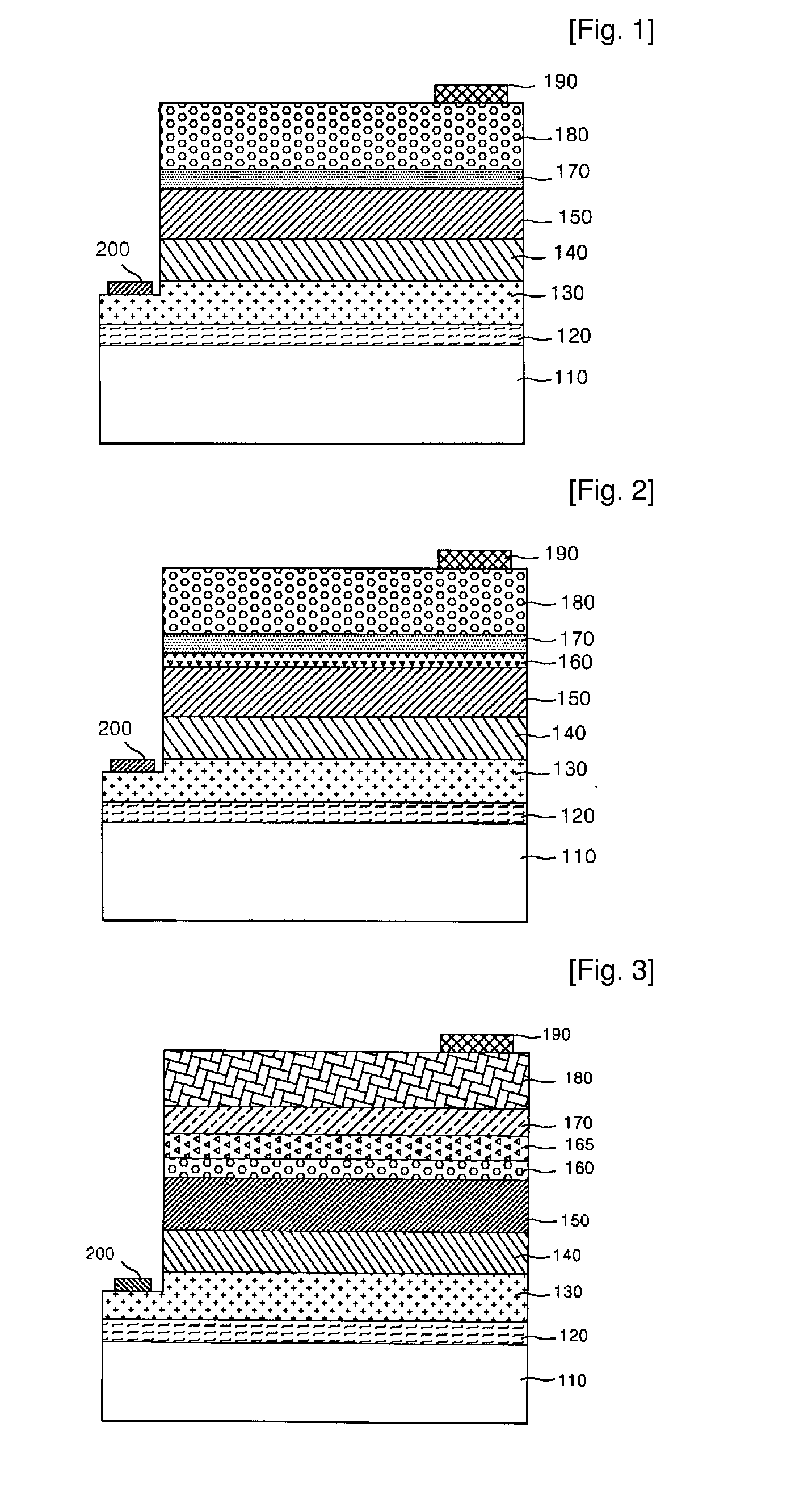
[0111]FIG. 3 shows a cross-sectional view of a flip-chip nitride-based light emitting device in accordance with the present invention. For elements having the same function as in the previously shown drawing, like numbers refer to like elements hereinafter.

[0112]Referring now to FIG. 3, the flip-chip light emitting device is formed of a structure including a substrate 110, a buffer layer 120, an n-type clad layer 130, an active layer 140, a p-type clad layer 150, an interface modification layer 160, an insert metal layer 165, a transparent conductive thin film layer 170 and a reflective layer 180 sequentially stacked thereon.

[0113]Herein, the interface modification layer 160, insert metal layer 165 and transparent conductive thin film layer 170 correspond to a multi-ohmic contact layer.

[0114]The insert metal layer 165 is formed between the interface modification layer 160 and transparent conductive thin film layer 170.

[0115]The insert metal layer 165 is preferably made up of a metal...

fourth embodiment

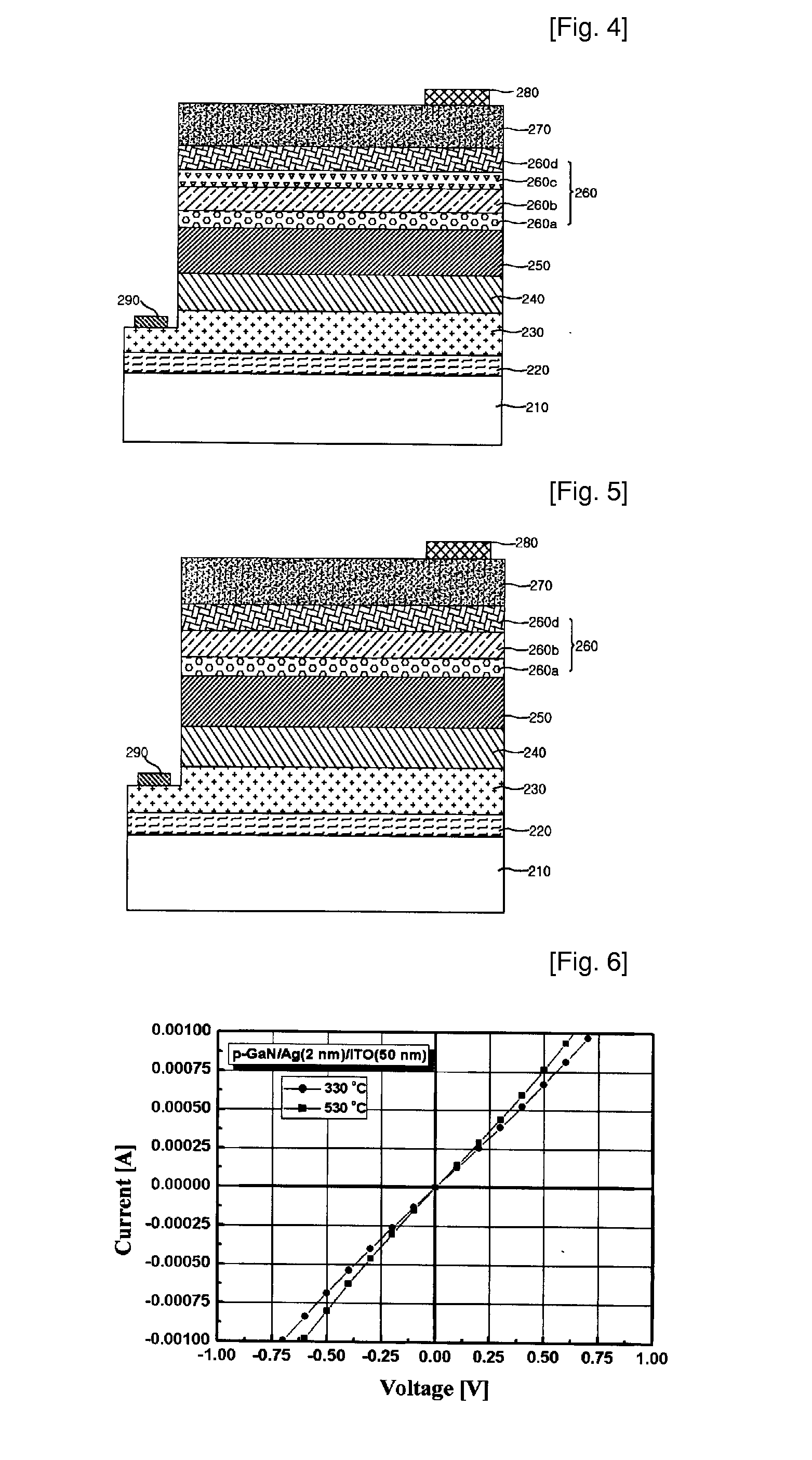
[0134]FIG. 4 shows a cross-sectional view of a flip-chip light emitting device in accordance with the present invention. Referring now to FIG. 4, the flip-chip light emitting device is formed of a structure including a substrate 210, a buffer layer 220, an n-type clad layer 230, an active layer 240, a p-type clad layer 250, a multi-ohmic contact layer 260 and a reflective layer 270 sequentially stacked thereon. Reference numerals 280 and 290 represent a p-type electrode pad and an n-type electrode pad, respectively.

[0135]Since the constituents of such a flip-chip light emitting device are substantially the same as in the first embodiment, except for the multi-ohmic contact layer 260, the detailed description thereof will be omitted. Hereinafter, the multi-ohmic contact layer 260 will be described.

[0136]The multi-ohmic contact layer 260 is formed by repeatedly stacking an interface modification layer 260a / transparent conductive thin film layer 260b as a stack unit. An example of such...


PUM

PropertyMeasurementUnit
thicknessaaaaaaaaaa
thicknessaaaaaaaaaa
thicknessaaaaaaaaaa

Abstract

Provided are a flip-chip nitride-based light emitting device having an n-type clad layer, an active layer and a p-type clad layer sequentially stacked thereon, comprising a reflective layer formed on the p-type clad layer and at least one transparent conductive thin film layer made up of transparent conductive materials capable of inhibiting diffusion of materials constituting the reflective layer, interposed between the p-type clad layer and reflective layer; and a process for preparing the same. In accordance with the flip-chip nitride-based light emitting device of the present invention and a process for preparing the same, there are provided advantages such as improved ohmic contact properties with the p-type clad layer, leading to increased wire bonding efficiency and yield upon packaging the light emitting device, capability to improve luminous efficiency and life span of the device due to low specific contact resistance and excellent current-voltage properties.

Description

TECHNICAL FIELD[0001]The present invention relates to a flip-chip nitride-based light emitting device and a process for preparing the same. More specifically, the present invention relates to a flip-chip nitride-based light emitting device having an electrode structure capable of improving luminous efficiency and a process for preparing the same.BACKGROUND ART[0002]Ohmic contact structures between semiconductors and electrodes are very important in realization of light emitting devices such as light emitting diodes (LEDs) and laser diodes (LDs), utilizing nitride-based compound semiconductors, for example gallium nitride (GaN) semiconductors emitting blue and green light and UV light. At present, commercially available gallium nitride-based light emitting devices are primarily formed on an insulating sapphire (Al2O3) substrate.[0003]Meanwhile, these gallium nitride-based light emitting devices are broadly divided into top-emitting light emitting diodes (TLEDs) and flip-chip light em...

Claims


Application Information

Patent Timeline
Patent Type & Authority Applications(United States)
IPC IPC(8): H01L33/00H01L21/329H01L33/10H01L33/20H01L33/32H01L33/42H01L33/62
CPCH01L33/405H01L33/32
Inventor SEONG, TAE-YEONSONG, JUNE-OKIM, KYOUNG-KOOKHONG, WOONG-KI
Owner SAMSUNG ELECTRONICS CO LTD
Why Eureka
Try Eureka