Circuit and methods for eliminating skew between signals in semiconductor integrated circuit

a technology of semiconductor integrated circuit and circuit, applied in the field of circuit and methods for eliminating skew between signals in semiconductor integrated circuit, can solve the problems of increasing circuit area, difficult to use cdr scheme in parallel communication scheme, and cdr scheme suffers from several limitations, so as to eliminate a skew, eliminate a per-data input/output pin skew

Active Publication Date: 2008-05-29
SAMSUNG ELECTRONICS CO LTD
View PDF7 Cites 9 Cited by
  • Summary
  • Abstract
  • Description
  • Claims
  • Application Information

AI Technical Summary

Benefits of technology

[0017]An aspect of the present disclosure includes a circuit for eliminating a skew between data and a clock signal in an interface between a semiconductor memory device and a memory controller. The circuit includes an edge information storage unit which stores edge information output from the semiconductor memory device, a pseudo data pattern generating unit which outputs pseudo data including a pattern similar to actually transmitted data, a phase detecting unit which receives the edge information from the edge information storage unit and the pseudo data from the pseudo data pattern generating unit to detect a phase difference between the data and the clock signal and generate a corresponding detection result, and a phase control unit which controls a phase of the clock signal according to the corresponding detection result from the phase detecting unit, so as to eliminate a per-data input/output pin skew in a data write and read operation of the semiconductor memory device.
[0018]Another aspect of the present disclosure includes a method for eliminating a skew between data and a clock signal in an interface between a semiconductor memory device and a memory controller. The me...

Problems solved by technology

While the above-mentioned features of a CDR scheme make it an attractive choice in the field of serial communications, the CDR scheme suffers from several limitations such as, for example, an increased circuit area.
Accordingly, the CDR scheme is difficult to use in a parallel communication scheme that is used in, for example, a DRAM.
While the per-pin skew calibration sch...

Method used


Image

  • Circuit and methods for eliminating skew between signals in semiconductor integrated circuit
  • Circuit and methods for eliminating skew between signals in semiconductor integrated circuit
  • Circuit and methods for eliminating skew between signals in semiconductor integrated circuit

Examples


Embodiment Construction

[0029]The present disclosure will now be described more fully hereinafter with reference to the accompanying drawings, in which exemplary embodiments of the invention are shown. This disclosure may, however, be embodied in different forms and should not be construed as limited to the embodiments set forth herein. Rather, these embodiments are provided as teaching examples of the disclosure.

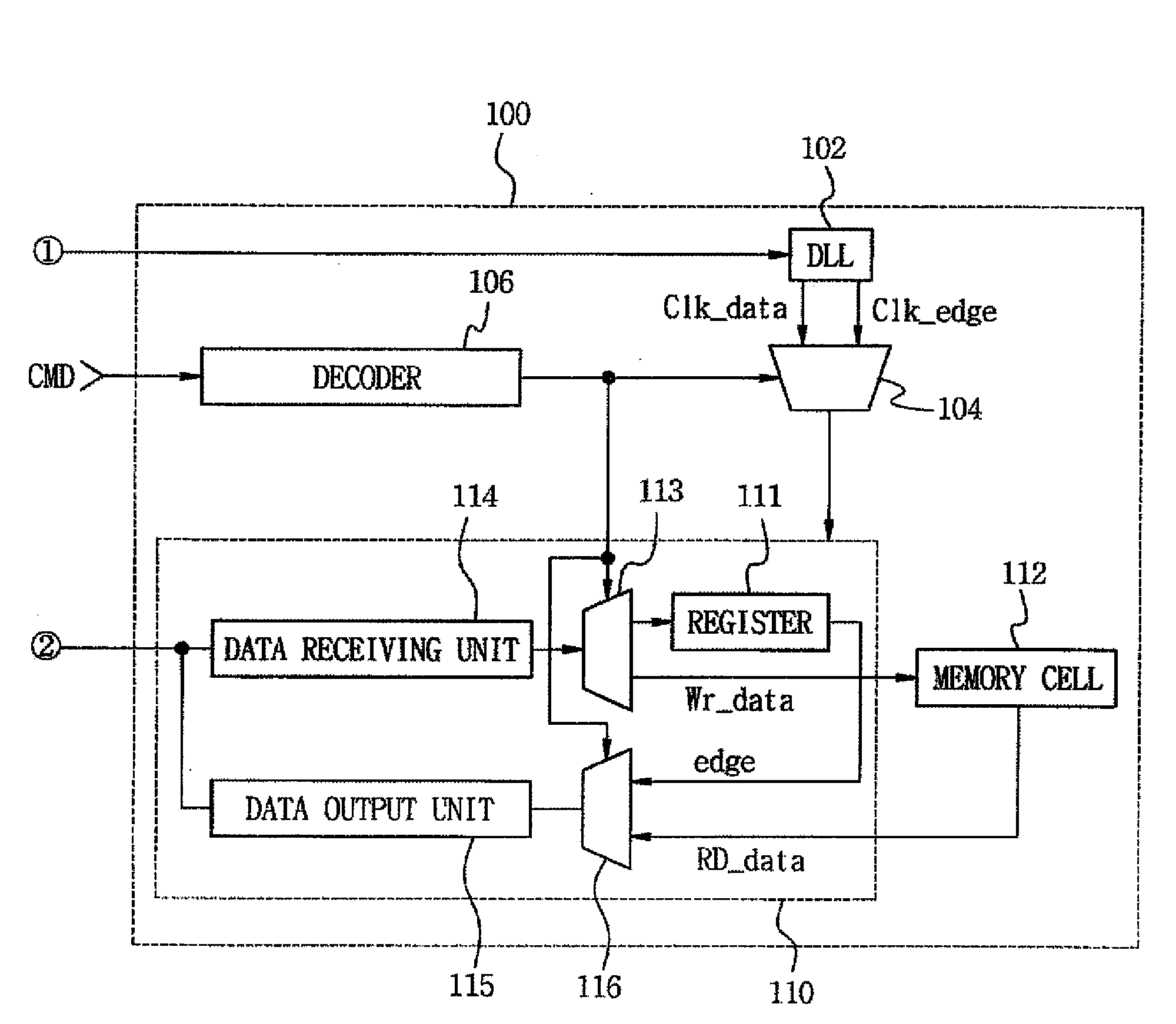
[0030]The present disclosure relates to a circuit for eliminating a skew between a clock signal and data and a method for eliminating the skew by using the same. More particularly, the present disclosure relates to a per-pin circuit for eliminating a skew and a method for eliminating a skew. Herein, the terms “eliminate”, “eliminating”, and variations thereof are intended to encompass both substantial reduction in skew and complete reduction in skew.

[0031]FIG. 3 is a block diagram illustrating a system including a skew eliminating circuit which eliminates a skew between data and a clock signal acc...


PUM


Abstract

A circuit for eliminating a skew between data and a clock signal in an interface between a semiconductor memory device and a memory controller includes an edge information storage unit which stores edge information output from the semiconductor memory device, a pseudo data pattern generating unit which outputs pseudo data including a pattern similar to actually transmitted data, a phase detecting unit which receives the edge information from the edge information storage unit and the pseudo data from the pseudo data pattern generating unit to detect a phase difference between the data and the clock signal and generate a corresponding detection result, and a phase control unit which controls a phase of the clock signal according to the corresponding detection result from the phase detecting unit, so as to eliminate a per-data input/output pin skew in a data write and read operation of the semiconductor memory device.

Description

CROSS-REFERENCE TO RELATED APPLICATION[0001]A claim of priority is made to Korean Patent Application No. 10-2006-0060285, filed Jun. 30, 2006, the disclosure of which is hereby incorporated herein by reference in its entirety.BACKGROUND OF THE INVENTION[0002]1. Technical Field[0003]The present disclosure relates to a semiconductor integrated circuit, and, more particularly, to a semiconductor integrated circuit which reduces a skew between data and a clock signal, and a method for eliminating a skew by using the same.[0004]2. Discussion of Related Art[0005]In serial communication schemes, communication circuits transmit the clock signal together with the data signals. On the other hand, in parallel communication schemes, communication circuits transmit the clock signal separately from the data.[0006]Because the serial communication schemes transmit the clock signal along with the data, a serial interface on the receiving end uses a clock data recovery scheme (“CDR”) to extract the c...

Claims


Application Information

Patent Timeline
IPC IPC(8): G11C7/02
CPCG11C5/063G11C7/02G11C7/1006G11C7/1051G11C7/222G11C7/1078G11C7/1087G11C7/22G11C7/106G11C7/10
Inventor BAE, SEUNG-JUNPARK, KWANG-ILJANG, SEONG-JIN
Owner SAMSUNG ELECTRONICS CO LTD
Why Eureka
Try Eureka