Transistor Device Formed on a Flexible Substrate Including Anodized Gate Dielectric

a technology of anodized gate dielectric and flexible substrate, which is applied in the direction of semiconductor devices, basic electric elements, electrical equipment, etc., can solve the problems of deformation of the substrate, current limitations of using flexible substrates, and material from which the flexible substrates are formed cannot withstand typical high temperature deposition processes

Inactive Publication Date: 2008-06-12
PALO ALTO RES CENT INC
View PDF11 Cites 11 Cited by
  • Summary
  • Abstract
  • Description
  • Claims
  • Application Information

AI Technical Summary

Benefits of technology

[0015]Accordingly, the present invention is directed to a method of forming, and structure so formed, operable as a thin film transistor. More particularly, the present invention is directed to a gate dielectric formed by a low temperature (e.g., at or below 150° C.) process. The method, and the structure so produced, is compatible with flexible substrates, enabling the production of, for example, flexible display and sensor arrays. A novel flexible display and a novel flexible sensor array are thus enabled.

Problems solved by technology

Many of the current limitations on using flexible substrates originate with the process requirements and structures of the devices, such as the thin-film transistors (TFTs), which comprise the backplane.
Unfortunately, the material from which the flexible substrates are formed cannot withstand typical high temperature deposition processes.
Furthermore, typical dielectric layers formed by higher temperature processes exhibit high intrinsic mechanical stress, which deforms the substrate and makes alignment for subsequent processing steps difficult.
There have been efforts to develop deposition processes compatible with flexible substrates, but such efforts have heretofore failed to produce effective results.
However, dielectric layers formed by these processes have typically been of poor quality and exhibit poor performance, for example due to a high density of pin holes, excessive leakage currents, etc.
Efforts to address the quality of the dielectric layers, for example by forming a relatively dense or thick dielectric layer have proved inadequate since as the density or thickness of the dielectric layer increases, so does the mechanical stress within the layer, resulting in deformation of the substrate and difficulty with alignment for subsequent processing steps.
Furthermore, obtaining proper operating capacitance of the gate dielectric limits the thickness of the dielectric layer.
Another impediment associated with using a flexible substrate is surface roughness.
Forming an organic semiconductor on a rough base results in ineffective polymer self-organization, and hence poor mobility and degraded device performance.
However, such a thick dielectric introduces the aforementioned stress and thickness-based capacitance issues, as well as so-called step coverage problems (e.g., non-uniform layer thicknesses at top, side, and corner of gate electrode), and the associated difficulties with controlling parasitic capacitances and shorts.

Method used


Image

  • Transistor Device Formed on a Flexible Substrate Including Anodized Gate Dielectric
  • Transistor Device Formed on a Flexible Substrate Including Anodized Gate Dielectric
  • Transistor Device Formed on a Flexible Substrate Including Anodized Gate Dielectric

Examples


first embodiment

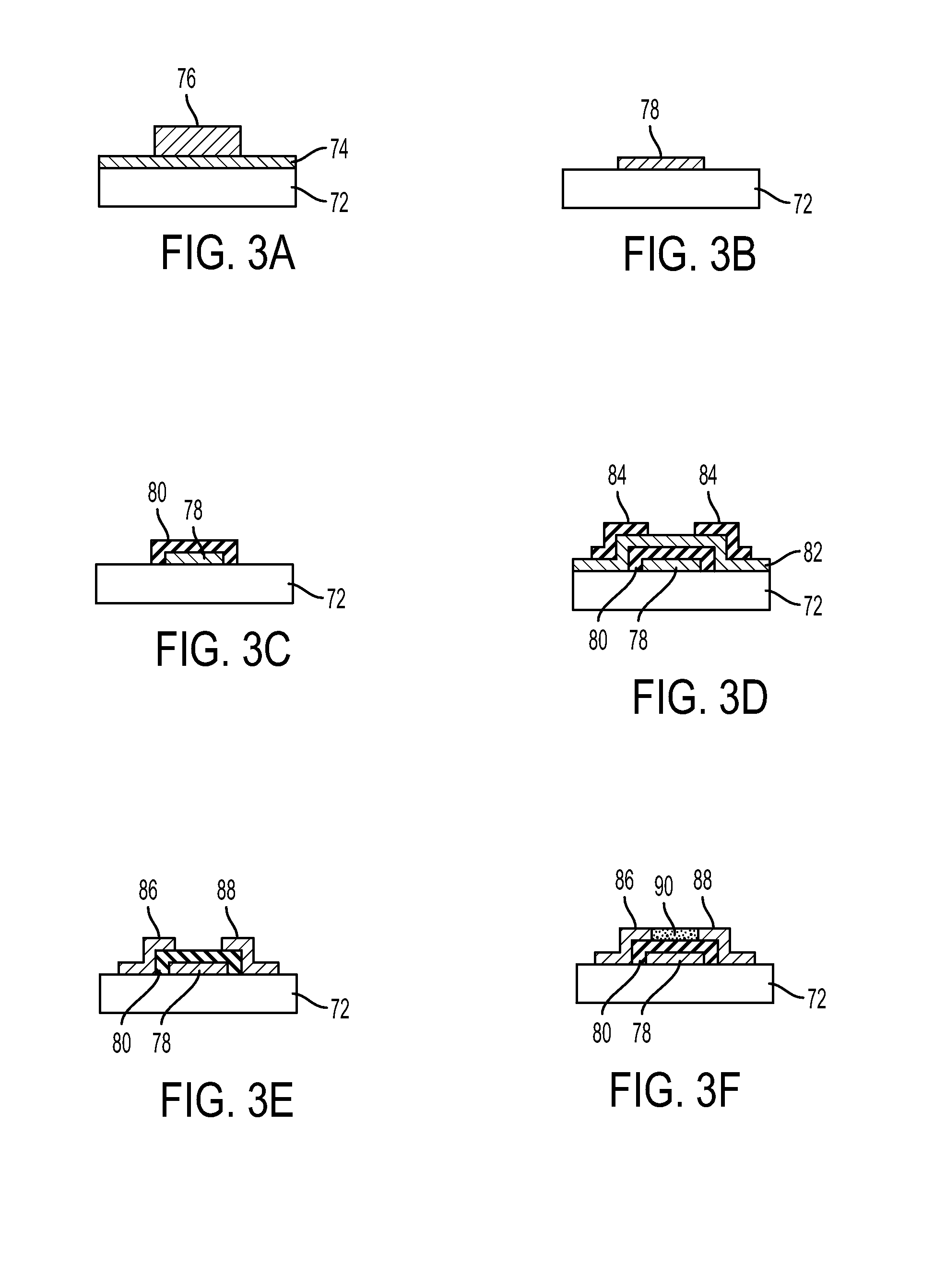
[0033]According to the present invention, illustrated in FIGS. 3a-3f, a TFT structure stack 70 is formed over a flexible substrate 72. Flexible substrate 72 may be a plastic film such as polyethylene naphthalate (PEN) polyethylene teraphlalate (PET), or a metal foil such as steel or even a thin glass sheet. Initially, a layer 74 of tantalum is deposited over substrate 72 by sputtering or thermal evaporation. Mask 76 is then formed over tantalum layer 74, for example by conventional photolithography or print patterning techniques such as those taught by Wong et al. in U.S. non-provisional patent application Ser. No. 11 / 193,847 (referred to as Wong et.), and the references cited therein (including U.S. Pat. Nos. 6,742,884 and 6,872,320), each of which being incorporated by reference herein. The structure is then etched, using mask 76 to protect a region of layer 74 thereunder, to thereby define a tantalum gate structure 78, as shown in FIG. 3b.

[0034]As an alternative to the process s...

second embodiment

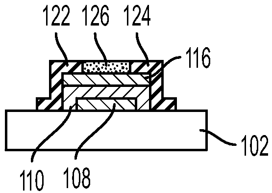
[0046]Accordingly, pursuant to the present invention, a second dielectric layer is formed over the Ta2O5 dielectric layer of the prior embodiment. With reference to FIGS. 8a-8g, the process for forming such a structure is shown. With reference first to FIG. 8, a TFT structure stack 100 is formed over a flexible substrate 102. Flexible substrate 102 may be a plastic film or other material as discussed above. A layer 104 of tantalum is deposited over substrate 102. Mask 106 is then formed over tantalum layer 104, for example by a print patterning technique. The structure is then etched, using mask 106 to protect the region of layer 104 thereunder, to thereby define a tantalum gate structure 108, as shown in FIG. 9. The aforementioned aluminum / tantalum combination may also be employed in the present embodiment, if required.

[0047]With reference now to FIG. 10, the in-process structure is then anodized to form a dielectric layer 110 of Ta2O5 over tantalum gate structure 108. The thicknes...

third embodiment

[0060]In the description associated with FIGS. 14 through 16, it was assumed that the optional step of etching the continuous layers such that the layer coverage over the substrate was minimized was performed. Similarly, the step of etching the continuous layers such that the layer coverage over the substrate is minimized is also optional for this However, for the following description we will assume that this optional etching has not been performed, with it being understood that similar steps may be performed and results obtained with or without this optional etching.

[0061]With reference next to FIG. 25, source / drain electrode metal layer 150 is formed over layer 146, and source / drain masking structures 152 are formed over layer 150, again for example by conventional photolithography of print patterning techniques such as those taught by Wong et al. The source / drain metal may be Cr, TiW, Al or another convenient metal. The structure is then etched to remove portions of the source / ...


PUM


Abstract

A transistor device is formed on a flexible substrate such that device processing remains at a low temperature. A first gate dielectric layer is formed over gate metal by annodization, eliminating relatively high-temperature dielectric deposition processes and difficulties with in-process substrate deformation. A second gate dielectric layer may optionally be provided over the first in order to provide an improved dielectric/semiconductor interface. A high performance pixel, and process for producing same, may thus be provided on a flexible substrate.

Description

STATEMENT REGARDING FEDERALLY SPONSORED RESEARCH AND DEVELOPMENT[0001]The U.S. Government has a fully paid-up license in this invention and the right in limited circumstances to require the patent owner to license others on reasonable terms as provided for by the terms of contract number 70NANB3H3029 awarded by the Department of Commerce, Advanced Technology Program.BACKGROUND OF THE INVENTION[0002]1. Field of the Invention[0003]The present invention relates to transistor devices formed on flexible substrates, and more specifically to a device including a first dielectric layer formed by anodizing a patterned metal, with an optional subsequently formed second dielectric layer thereover.[0004]2. Description of the Prior Art[0005]There exists today many types and techniques for fabricating flat-panel display devices, for example of the type used as a computer display, television monitor, etc. For the purposes herein, the term “display” will generically encompass all such devices. Disp...

Claims


Application Information

Patent Timeline
Patent Type & Authority Applications(United States)
IPC IPC(8): H01L29/76
CPCH01L21/31683H01L29/4908H01L51/055H01L51/0097H01L51/0525H01L29/7869H10K10/472H10K10/481H10K77/111H01L21/02244
Inventor ARIAS, ANA CLAUDIALUJAN, RENESTREET, ROBERT
Owner PALO ALTO RES CENT INC
Why Eureka
Try Eureka