Nonvolatile semiconductor memory device and method for manufacturing the same

a semiconductor memory and non-volatile technology, applied in the direction of semiconductor devices, basic electric elements, electrical appliances, etc., can solve the problems of large stress in the tunnel insulating film, increased leakage current, degraded data retention characteristics, etc., and achieve the effect of reducing stress-induced leakage current and low program voltag

Active Publication Date: 2008-06-12
KIOXIA CORP
View PDF12 Cites 17 Cited by
  • Summary
  • Abstract
  • Description
  • Claims
  • Application Information

AI Technical Summary

Benefits of technology

[0013]The present invention has been made in view of these circumstances, and an object thereof is to provide a nonvolatile semiconductor memory device that can lower the program voltage while reducing the stress-induced leakage current, and a method for manufacturing such a nonvolatile semiconductor memory device.

Problems solved by technology

In such a case, a high voltage is required for injecting and pulling electrons into and out of the floating gate electrode, and large stress is caused in the tunnel insulating film.
As a result, defects such as traps are formed in the tunnel insulating film, and the leakage current (stress-induced leakage current) increases and degrades the data retention characteristics and the likes.
The defects in the tunnel insulating film that cause the leakage current are formed, because a large amount of energy is generated due to the voltage application when the electrons in the silicon atoms tunnel through the conduction band of the tunnel insulating film to the cathode side.
More specifically, when the tunneling electrons having the energy depending on the applied voltage move to the cathode side, impact ions are generated on the cathode side, and holes with a large amount of energy are generated or the hydrogen bonding existing in the silicon interfaces is cut off by the impact ions, resulting in the defects in the tunnel insulating film.
The defects then cause leakage current and insulation breakdown.
Where the devices are made smaller, the electric field to be induced into the interelectrode insulating film becomes larger, and causes a serious problem in reliability, unless the program voltage can be lowered.
In this manner, the thickness reduction and the reliability are in a trade-off relationship, which is a significant cause of the hindrance to a decrease in film thickness of the tunnel oxide film.
As described above, there is the trade-off problem with a nonvolatile semiconductor memory device such as an EEPROM in which a reduction of the film thickness of the tunnel insulating film is effective in lowering the program voltage, but traps are formed when a high voltage is applied at the time of writing / erasing, resulting in an increase in leakage current.
However, it has been very difficult to satisfy such demand by conventional techniques.

Method used


Image

  • Nonvolatile semiconductor memory device and method for manufacturing the same
  • Nonvolatile semiconductor memory device and method for manufacturing the same
  • Nonvolatile semiconductor memory device and method for manufacturing the same

Examples


first embodiment

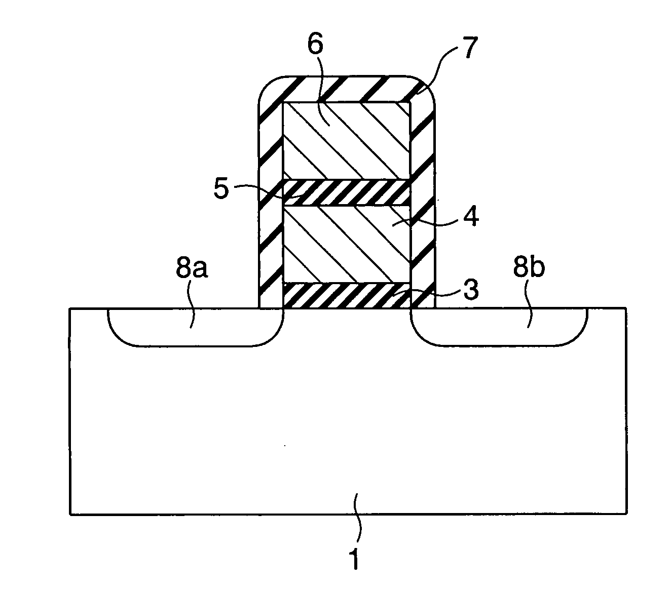
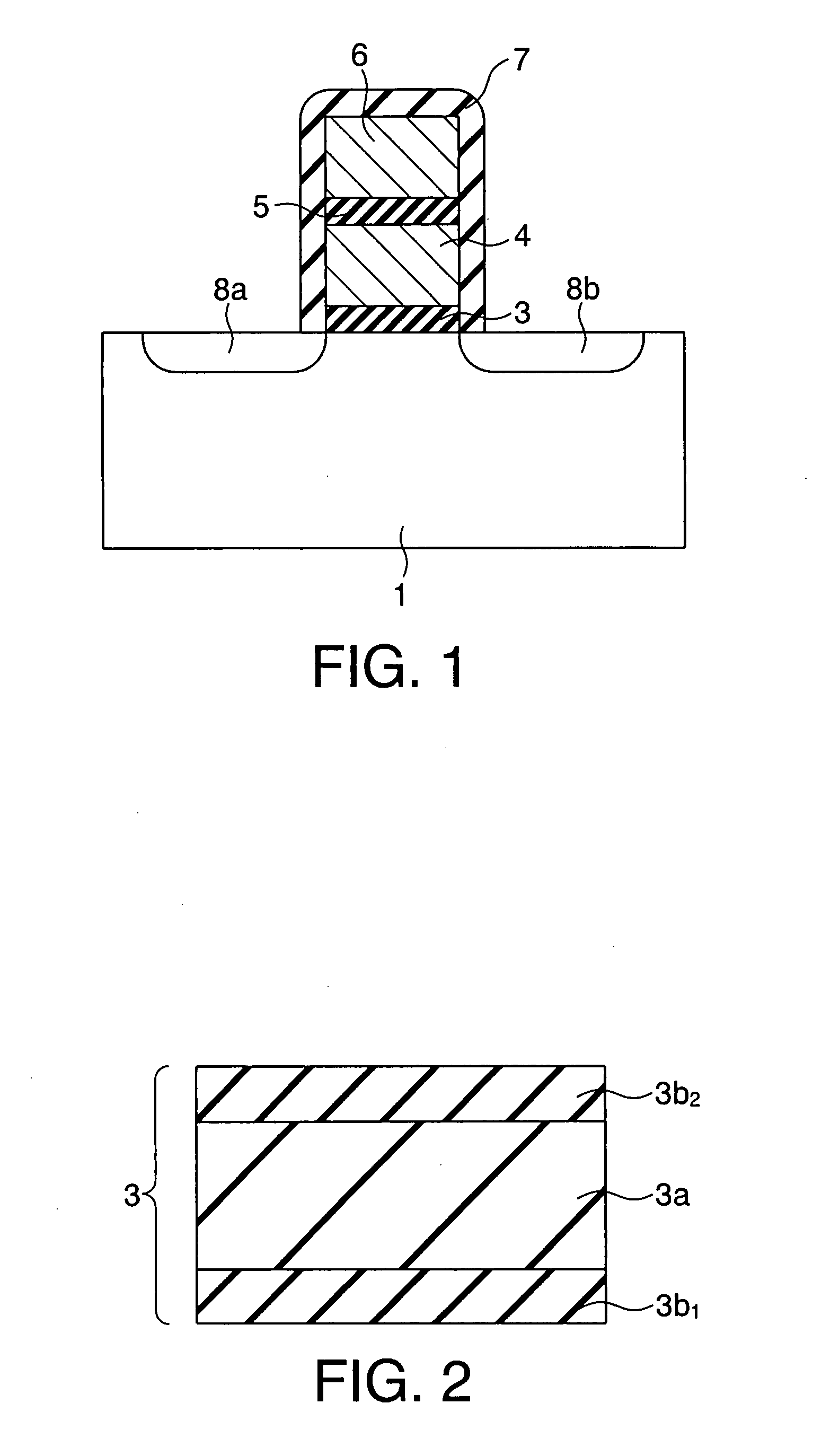
[0045]A nonvolatile semiconductor memory device in accordance with a first embodiment of the present invention includes NAND cell units arranged in a matrix form. Each of the NAND cell units includes a NAND cell formed with memory cells connected in series. Each of the memory elements has an n-type source region 8a and drain region 8b formed at a distance from each other on a p-type silicon substrate 1, as shown in FIG. 1. The n-type source region 8a and drain region 8b contain n-type impurities (such as phosphorus). A tunnel insulating film 3 is formed on a portion of the silicon substrate 1 located between the source region 8 and drain region 8b. A floating gate electrode 4 is formed on the tunnel insulating film 3. An interelectrode insulating film 5 is formed on the floating gate electrode 4. A control gate electrode 6 is formed on the interelectrode insulating film 5. The tunnel insulating film 3, the floating gate electrode 4, the interelectrode insulating film 5, and the cont...

second embodiment

[0080]Referring now to FIG. 22A through FIG. 23D, a method for manufacturing a nonvolatile semiconductor memory device in accordance with a second embodiment of the present invention is described.

[0081]First, as shown in FIG. 22A, a p-type silicon substrate 1 with a plane orientation (100) and resistivity of 10 to 20 Ωcm is prepared, and a silicon oxide layer 3b1 containing germanium, for example, is formed on the surface of the p-type silicon substrate 1. A silicon oxide layer 3a not containing germanium is then formed, as shown in FIG. 22B. A silicon oxide layer 3b2 containing germanium is then stacked, as shown in FIG. 22C. In this manner, a tunnel insulating film 3 having a layer including an injection assisting level of germanium at either interface is completed, as shown in FIG. 22D. Although the tunnel insulating film 3 is formed with silicon oxide layers in this embodiment, it is possible to employ silicon nitride layers or silicon oxynitride layers, instead of the silicon o...

third embodiment

[0092]Referring now to FIG. 25A through FIG. 26B, a method for manufacturing a MONOS (Metal-Oxide-Nitride-Oxide-Silicon)-type or SONOS (Silicon-Oxide-Nitride-Oxide-Silicon)-type nonvolatile semiconductor memory device in accordance with a third embodiment of the present invention is described.

[0093]First, the procedures in accordance with the second embodiment are carried out, up to the point where the tunnel insulating film that has the layers including the injection assisting levels formed with germanium at both interfaces is formed. A 10-nm thick silicon nitride film 9 is then formed as a charge storage layer on the tunnel insulating film 3, with the use of a mixed gas of a NH3 gas and a SiH2Cl2 or Si2Cl6 gas, as shown in FIG. 25A.

[0094]A 15-nm thick block insulating film layer 10 is then formed on the silicon nitride film 9, as shown in FIG. 25B. This block insulating film layer 10 is formed by depositing a silicon oxide film by CVD method, for example.

[0095]A conductor layer 6 ...


PUM


Abstract

A nonvolatile semiconductor memory device includes: a memory element, the memory element including: a semiconductor substrate; a first insulating film formed on a region in the semiconductor substrate located between a source region and a drain region, and having a stack structure formed with a first insulating layer, a second insulating layer, and a third insulating layer in this order, the first insulating layer including an electron trapping site, the second insulating layer not including the electron trapping site, and the third insulating layer including the electron trapping site, and the electron trapping site being located in a position lower than conduction band minimum of the first through third insulating layers while being located in a position higher than conduction band minimum of a material forming the semiconductor substrate; a charge storage film formed on the first insulating film; a second insulating film formed on the charge storage film; and a control gate electrode formed on the second insulating film.

Description

CROSS-REFERENCE TO RELATED APPLICATION[0001]This application is based upon and claims the benefit of priority from prior Japanese Patent Application No. 2006-332313 filed on Dec. 8, 2006 in Japan, the entire contents of which are incorporated herein by reference.BACKGROUND OF THE INVENTION[0002]1. Field of the Invention[0003]The present invention relates to a nonvolatile semiconductor memory device and a method for manufacturing the nonvolatile semiconductor memory device.[0004]2. Related Art[0005]In recent years, memory elements have been rapidly becoming smaller in nonvolatile semiconductor memory devices such as EEPROMs (Electrically Erasable and Programmable Read Only Memories) in which writing and erasing can be electrically performed. In a case of an EEPROM, a high voltage is applied to the control gate electrode, so that electrons are injected into the floating gate electrode from the substrate side through a tunnel insulating film containing silicon (writing), or electrons a...

Claims


Application Information

Patent Timeline
Patent Type & Authority Applications(United States)
IPC IPC(8): H01L29/792H01L21/336
CPCH01L21/28273H01L21/28282H01L29/792H01L29/513H01L29/7881H01L29/42324H01L29/40114H01L29/40117H01L29/4234
Inventor MITANI, YUICHIROKOIKE, MASAHIRONAKASAKI, YASUSHIMATSUSHITA, DAISUKE
Owner KIOXIA CORP
Why Eureka
Try Eureka