Compact light conversion device and light source with high thermal conductivity wavelength conversion material

a wavelength conversion material and light conversion technology, applied in the direction of semiconductor devices, electrical devices, photovoltaics, etc., can solve the problems of significant local heating within the wavelength conversion material, thermal quenching of the wavelength conversion and light emission, and subsequent reduction of the emitted light flux, so as to facilitate the formation of an electrical interconnection, reduce the amount of wavelength conversion elements, and reduce the effect of light outpu

Inactive Publication Date: 2008-06-26
GOLDENEYE
View PDF5 Cites 116 Cited by
  • Summary
  • Abstract
  • Description
  • Claims
  • Application Information

AI Technical Summary

Benefits of technology

[0014]Embodiments of this invention include at least one heat sink that is in direct thermal contact with the wavelength conversion element. Heat generated within the wavelength conversion element is dissipated quickly to the ambient environment in order to prevent the wavelength conversion element from overheating and undergoing thermal quenching of the wavelength conversion and light emission.
[0015]One embodiment of this invention is a wavelength conversion device that includes a wavelength conversion element that has an input surface and an output surface, a heat sink in thermal contact with the wavelength conversion element and an optional thermally conducting reflector interposed between the wavelength conversion element and the heat sink. The wavelength conversion element converts light of a first wavelength range into light of a second wavelength range. The second wavelength range is different than the first wavelength range. The wavelength conversion device may include additional elements such as a first dichroic mirror fabricated on or positioned near the output surface, a second dichroic mirror fabricated on or positioned near the input surface, light extraction elements fabricated on the output surface or an electrical connection fabricated on or embedded in the input surface. The electrical connection facilitates the formation of an electrical interconnection to a light-emitting device that is positioned adjacent to the input surface of the wavelength conversion device.
[0016]Another embodiment of this invention is a light source that includes a wavelength conversion element that has an input surface and an output surface, an LED positioned adjacent to the input surface and a heat sink in thermal contact with both the wavelength conversion element and the LED. The LED may or may not be in direct thermal contact with the wavelength conversion element. Preferably the LED and wavelength conversion element are not in direct thermal contact so that the wavelength conversion element will not overheat the LED and the LED will not overheat the wavelength conversion element. If the wavelength conversion element is overheated, thermal quenching may occur and the light output from the wavelength conversion element will be reduced. If the LED is overheated, the LED will become less efficient and the light output from the LED will drop. The wavelength conversion element can optionally include an electrical connection fabricated on or embedded in the input surface of the element. The electrical connection on the wavelength conversion device facilitates the formation of an electrical interconnection to the adjacent LED.
[0017]Other embodiments of this invention include two or more heat sinks to cool the device or light source. For example, one embodiment of this invention is a light source that includes a wavelength conversion element that has an input surface and an output surface, a first heat sink that is in thermal contact with the wavelength conversion element, an LED positioned adjacent to the input surface and a second heat sink in thermal contact with the LED. The first heat sink is not in direct thermal contact with the second heat sink. The LED may or may not be in direct thermal contact with the wavelength conversion element. Preferably the LED and wavelength conversion element are not in direct thermal contact so that the wavelength conversion element will not overheat the LED and the LED will not overheat the wavelength conversion element. The wavelength conversion element can optionally include an electrical connection fabricated on or embedded in the input surface of the element. The electrical connection on the wavelength conversion device facilitates the formation of an electrical interconnection to the adjacent LED.

Problems solved by technology

The conversion of an excitation wavelength into an emitted wavelength by a wavelength converting material is not 100 percent efficient.
For powdered phosphors, this can lead to a significant amount of local heating within the wavelength conversion material following exposure to the excitation light.
The heating is due to the lack of an adequate thermal conduction path from the phosphor powder grains to the ambient environment and can result in thermal quenching of the wavelength conversion and light emission and a subsequent reduction in the emitted light flux.
While the thermal quenching characteristics can be improved using alternate materials, some tradeoffs regarding light output efficiency or spectral content of the converted light are usually required.
Although such approaches are adequate for low levels of LED excitation, the lack of an adequate thermal conduction path to ambient limits the maximum light flux level one can use to excite the powdered phosphors.
Another disadvantage of using a powdered phosphor with a binder is that the high surface area of the powdered phosphor results in a variety of degradation mechanisms for both the phosphor and the binder.
For example, the binders that surround the phosphor particles, especially organic-based binders, tend to degrade and / or turn yellow under high light flux levels.
However, the approach of increasing the phosphor area or volume makes optical coupling inefficient in applications requiring a small source size or small source etendue.
In addition, increasing the phosphor area or volume also increases the overall size and weight of the LED source with a higher cost associated with the larger volume of the wavelength conversion material.
This deficiency in the phosphor-at-a-distance approach is at least partly driven by the lack of an efficient thermal conduction path for the wavelength conversion material.
Heat generated in the wavelength conversion layer must flow through the LED to get to the heat sink, thereby increasing the temperature of the LED and possibly lowering the light output of the LED.
Both heat flows can be tolerated in low-power devices, but will significantly reduce the performance of high-power devices.
However, some of the heat generated in the wavelength conversion layer will still flow through the LED to get to the heat sink, thereby increasing the temperature and possibly lowering the light output of the LED.
Both heat flows can be tolerated in low-power devices, but can significantly reduce the performance of high-power devices.
In addition, all the heat must still go through a single heat sink, which may not be able to handle the heat load for both the LED and the wavelength conversion layer in high-power devices.
However, Mueller et al. do not disclose the use of a thermally conducting monocrystalline wavelength conversion element or other non-ceramic element in direct thermal contact with a heat sink and do not disclose the use of two or more separate heat sinks for the luminescent ceramic and the LED.
Furthermore, Mueller et al. do not disclose physically separating the luminescent ceramic and the LED to prevent direct thermal contact between the two elements.
Having direct thermal contact between the LED and the luminescent ceramic and having only one heat sink for both elements may cause the luminescent ceramic to overheat the LED or cause the LED to overheat the luminescent ceramic in the Mueller et al.
Either type of overheating can result in a reduction in light output from the LED.

Method used


Image

  • Compact light conversion device and light source with high thermal conductivity wavelength conversion material
  • Compact light conversion device and light source with high thermal conductivity wavelength conversion material
  • Compact light conversion device and light source with high thermal conductivity wavelength conversion material

Examples


Embodiment Construction

[0031]The preferred embodiments of the present invention will be better understood by those skilled in the art by reference to the above listed figures. The preferred embodiments of this invention illustrated in the figures are not intended to be exhaustive or to limit the invention to the precise form disclosed. The figures are chosen to describe or to best explain the principles of the invention and its applicable and practical use to thereby enable others skilled in the art to best utilize the invention.

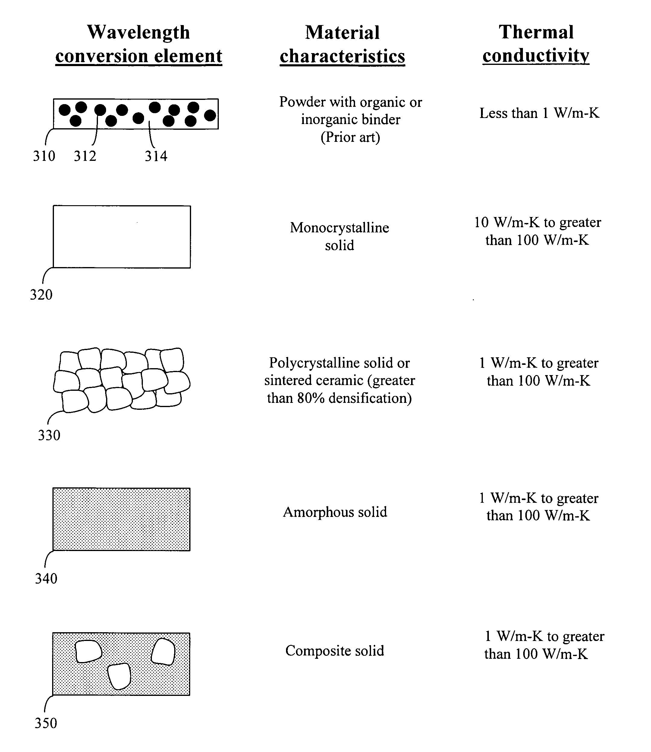
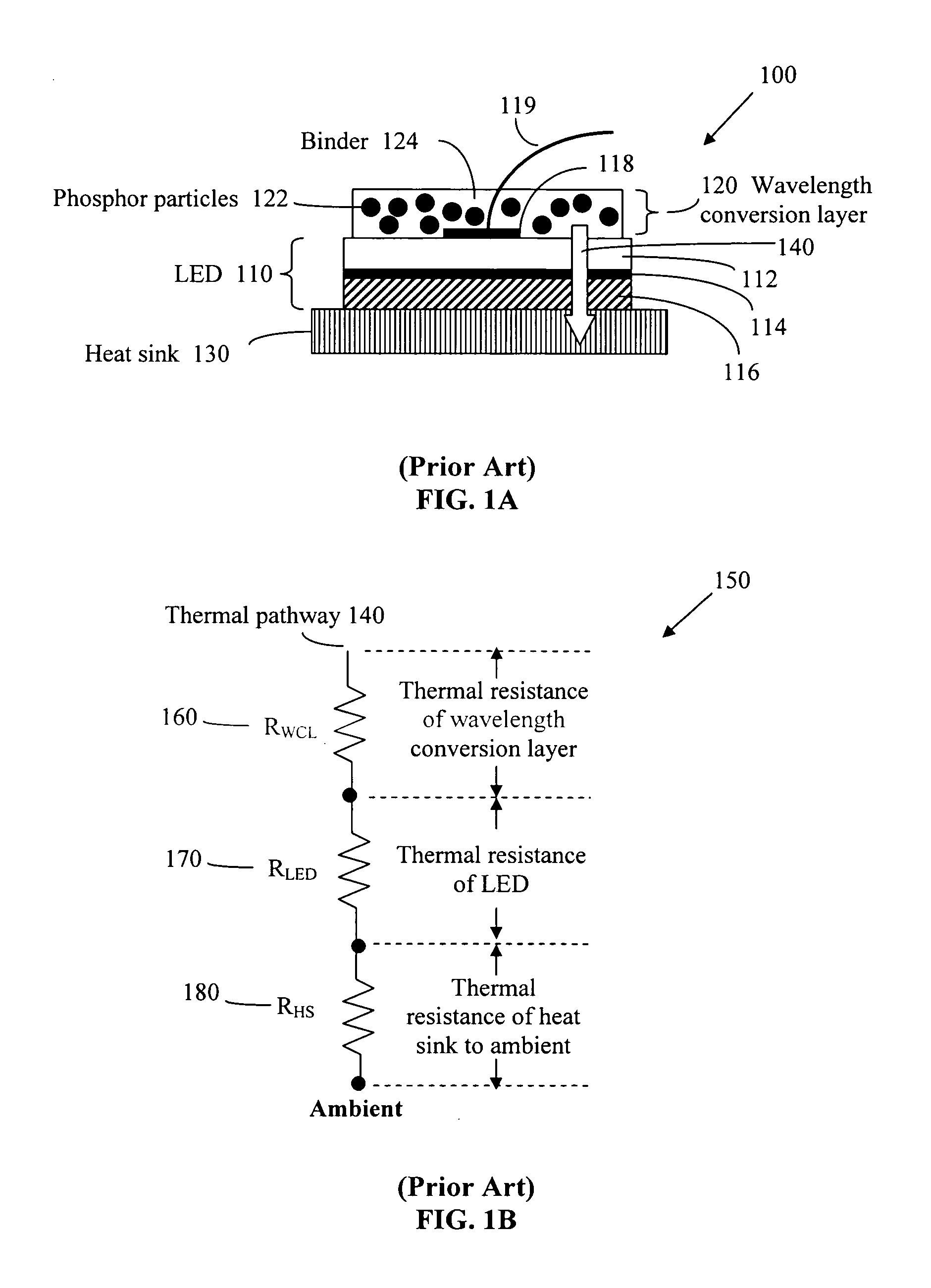
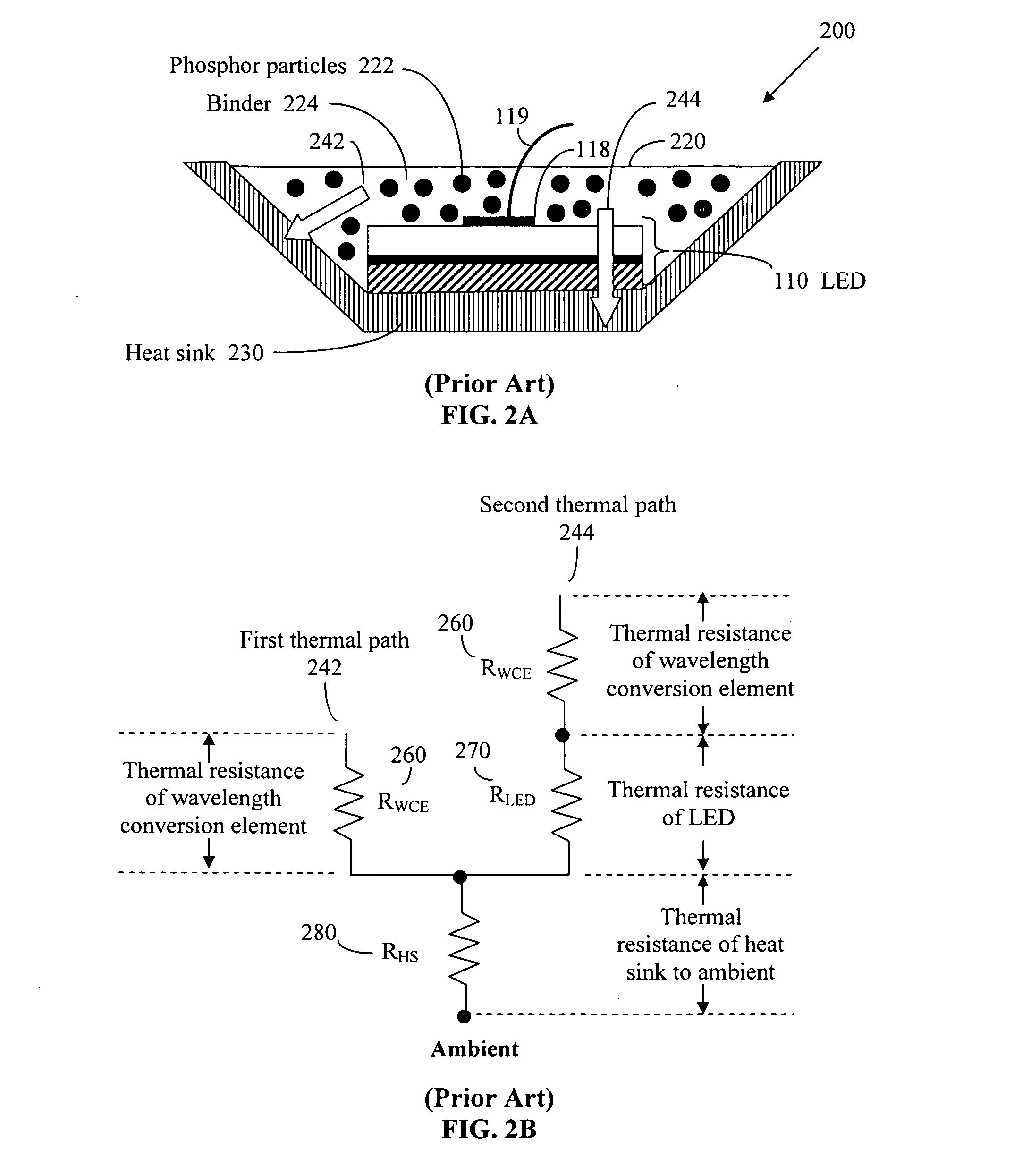
[0032]Compact, high-intensity light conversion devices and compact, high-intensity, solid-state light sources utilize wavelength conversion materials that preferably have a thermal conductivity greater than 1 watt per meter per degree Kelvin (W / m-K). Exemplary wavelength conversion materials are monocrystalline solids, polycrystalline solids, substantially densified ceramic solids, amorphous solids or composite solids. Substantially densified ceramics are ceramics that have prefer...


PUM

PropertyMeasurementUnit
reflectivityaaaaaaaaaa
particle sizesaaaaaaaaaa
reflectivityaaaaaaaaaa

Abstract

A light conversion device and high-intensity, solid-state light source utilize wavelength conversion elements with a thermal conductivity greater than 1 watt per meter per degree Kelvin (W/m-K). Exemplary materials that have high thermal conductivity include monocrystalline solids, polycrystalline solids, substantially densified ceramic solids, amorphous solids or composite solids. The light conversion device and high-intensity, solid-state light source have at least one heat sink that is in direct thermal contact with the wavelength conversion element. The heat sink quickly dissipates heat generated within the wavelength conversion element in order to prevent the wavelength conversion element from overheating and undergoing thermal quenching of the wavelength conversion and light emission.

Description

TECHNICAL FIELD[0001]The present invention is a light conversion device and light source that can be implemented using solid-state, light-emitting devices such as light emitting diodes (LEDs). The invention has a high thermal conductivity wavelength conversion material and also includes means for thermal cooling of such devices and light sources.BACKGROUND OF THE INVENTION[0002]Solid-state lighting has expanded rapidly based on the development of efficient inorganic and organic light emitting diode devices. These LED devices tend to be narrow band optical emitters that must be combined or coupled with wavelength conversion materials to create useful white light sources. In particular, wavelength conversion means such as powder phosphors are used to broaden or shift the emission bands of blue or ultraviolet (UV) LEDs. Powder based phosphors are typically created using solid-state processes. The phosphors are then combined with various binders such as organic materials or inorganic gl...

Claims


Application Information

Patent Timeline
Patent Type & Authority Applications(United States)
IPC IPC(8): H01L31/042
CPCH01L31/02322H01L31/024H01L31/052H01L33/501H01L2224/73265H01L33/644Y02E10/50H01L24/32H01L33/507H01L2924/12041H01L2924/12044H01L2924/00
Inventor BEESON, KARL W.ZIMMERMAN, SCOTT M.ROSS, RICHARD L.LIVESAY, WILLIAM R.
Owner GOLDENEYE
Why Eureka
Try Eureka