Process for Large-Scale Production of Cdte/Cds Thin Film Solar Cells, Without the Use of Cdci2
a technology of cdte/cds and solar cells, applied in the field of solar cell technology, can solve the problems of affecting the achievement of the target, affecting the stability of the target, and damage to the film, and achieve the effect of reducing production costs
- Summary
- Abstract
- Description
- Claims
- Application Information
AI Technical Summary
Benefits of technology
Problems solved by technology
Method used
Image
Examples
example
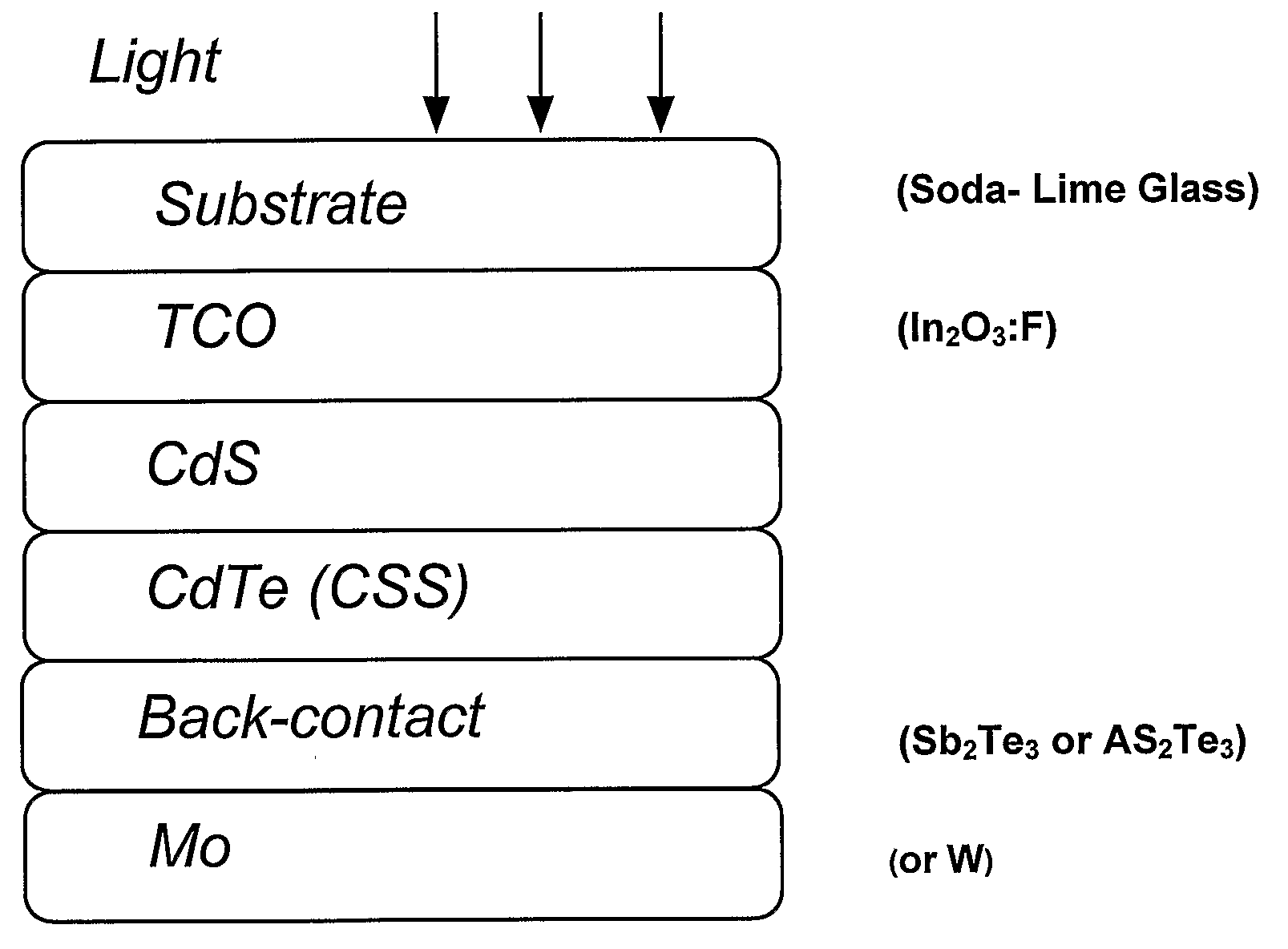
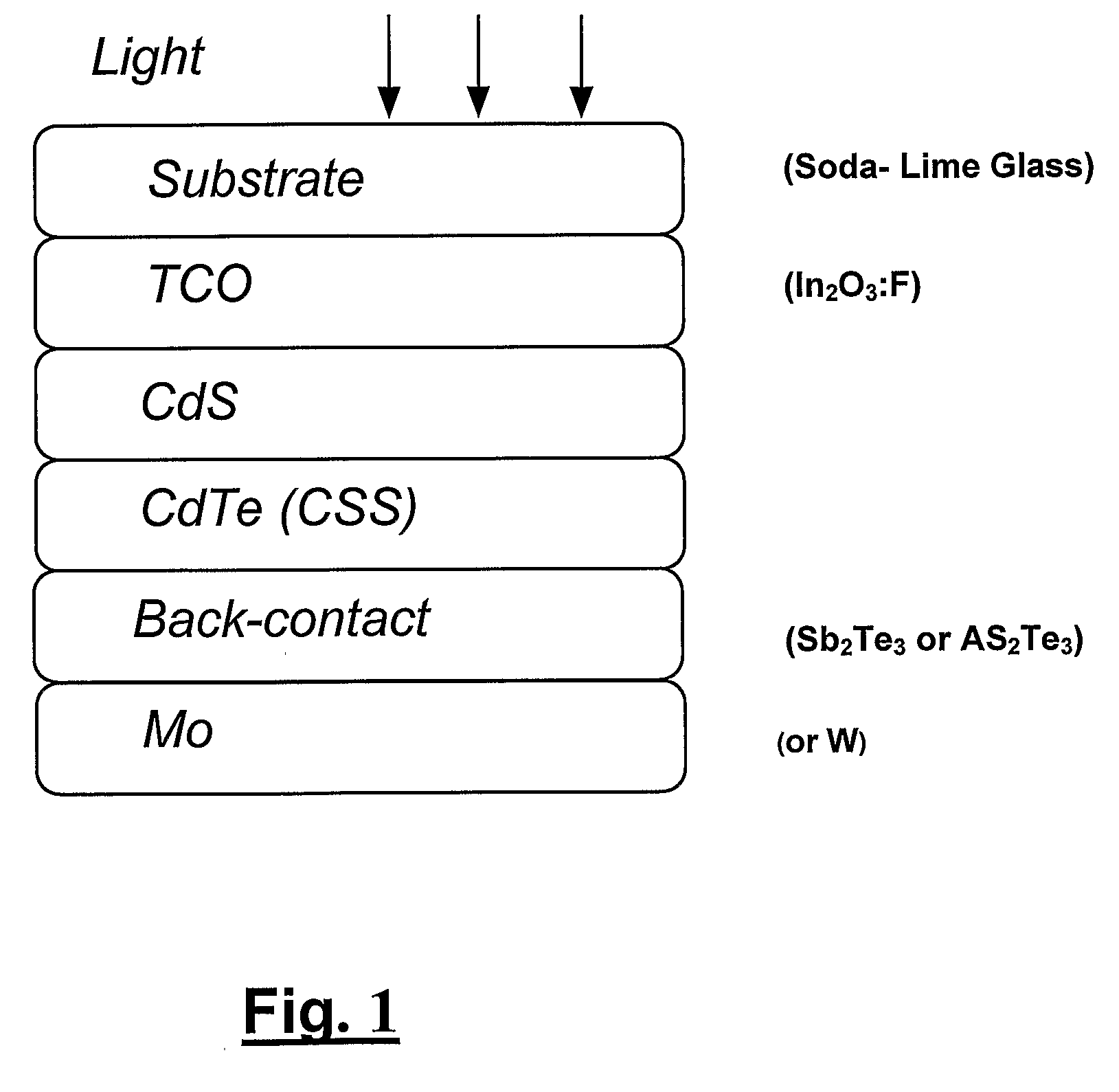
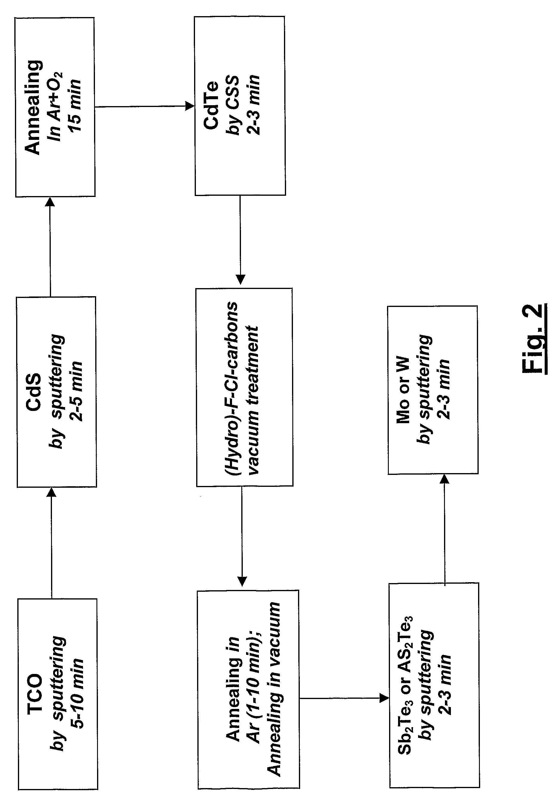
[0041]A cell exhibiting a 15% efficiency has been prepared in the following way: a soda-lime glass has been covered by 500 nm of In2O3:F (fluorine-doped) deposited at 500° C. substrate temperature as described above. 100 nm of CdS have been deposited by sputtering at 300° C. substrate temperature and annealed for 15 min at 500° C. in 500 mbar of Ar containing 20% of O2. 8 μm of CdTe have been deposited on top of CdS by CSS at a substrate temperature of 500° C. Both CdS and CdTe films are produced from a compact block source as described in WO03 / 032406. A treatment with HCF2Cl has been done in an Ar atmosphere as described above. Finally a back contact has been created, without any etching, by depositing in sequence by sputtering 150 nm of Sb2Te3 and 150 nm of Mo.
[0042]After one hour under 10 suns at a temperature of 180° C. in open-circuit conditions the solar cell prepared in this way exhibited the following parameters:
Voc860 mVJsc25.4 mA / cm2ff0.69efficiency15%
[0043]Similar results...
PUM
 Abstract
Description
Claims
Application Information


