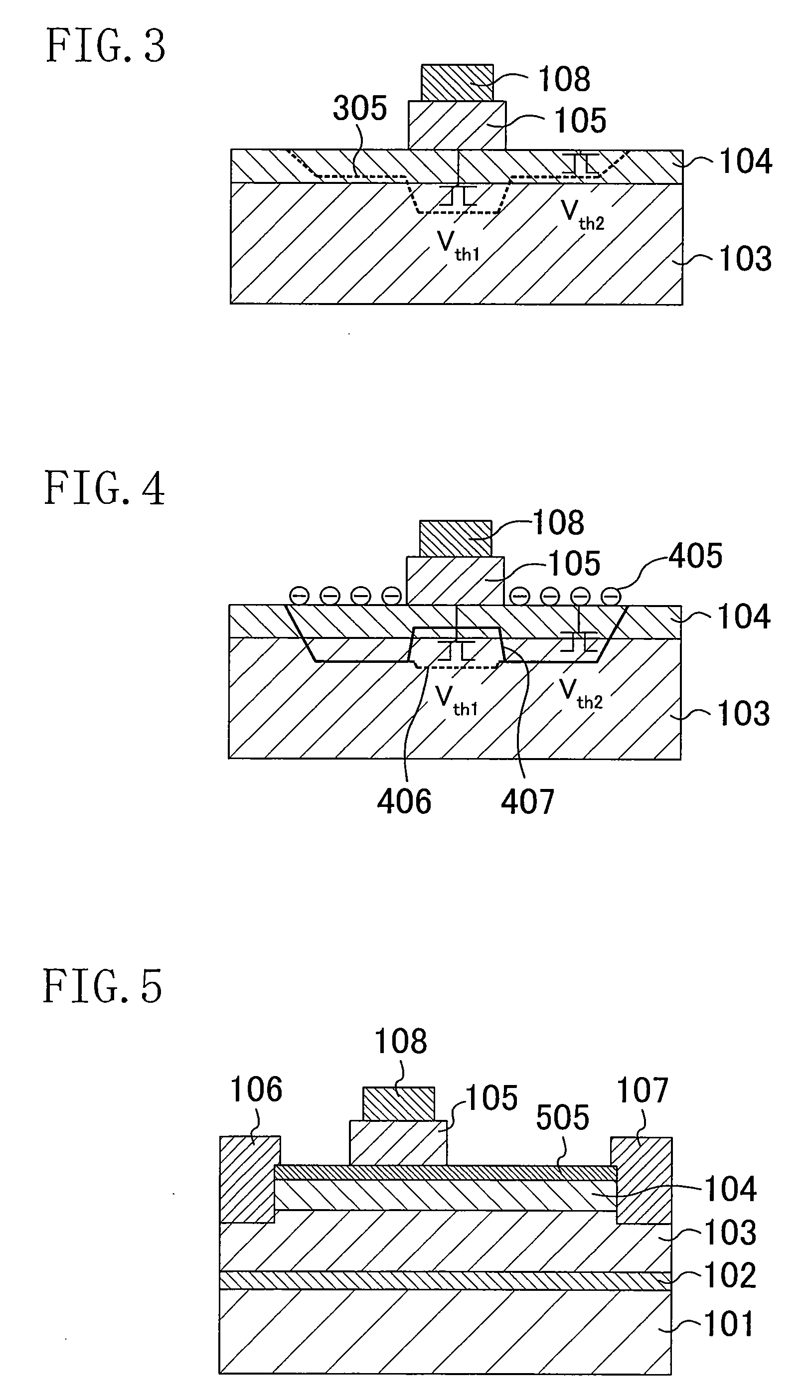
[0018]FIG. 6 is a sectional view showing expansion of a depletion layer in applying a drain
voltage to the transistor of the second comparative example of the present invention. In the transistor of the second comparative example, the transistor is set to an off-state with a drain
voltage as high as about 60 V applied thereto. In this case, as shown in FIG. 6, the
threshold voltage difference ΔVth described above is set to have an increased value, so that below the side of the gate
electrode 108, the depletion layer (the edge 607 of the depletion layer in the off-state) expands only to the location where a channel opens. With a drain
voltage applied in this state, when a positive voltage (3 V) is applied to the gate to turn into an on-state, a depletion layer (the edge 608 of the depletion layer in the on-state) created below the side of the gate electrode 108 is affected by electrons trapped in the
surface states. Therefore, this depletion layer is still kept in the state in which it expands, without changing from the off-state, to the location where a channel opens. In this condition, the state of the
drain current is determined by the location of the depletion layer created below the gate electrode 108. Therefore, in the transistor of the second comparative example, a sufficient
drain current can be observed even after application of a
high voltage thereto. Accordingly, with the transistor of the second comparative example, current collapse can be prevented. As is apparent from the above, a conceivable important point to prevent the current collapse is that the
threshold voltage below the side of the gate electrode 108 is made small enough to have a vale of a completely
negative voltage.
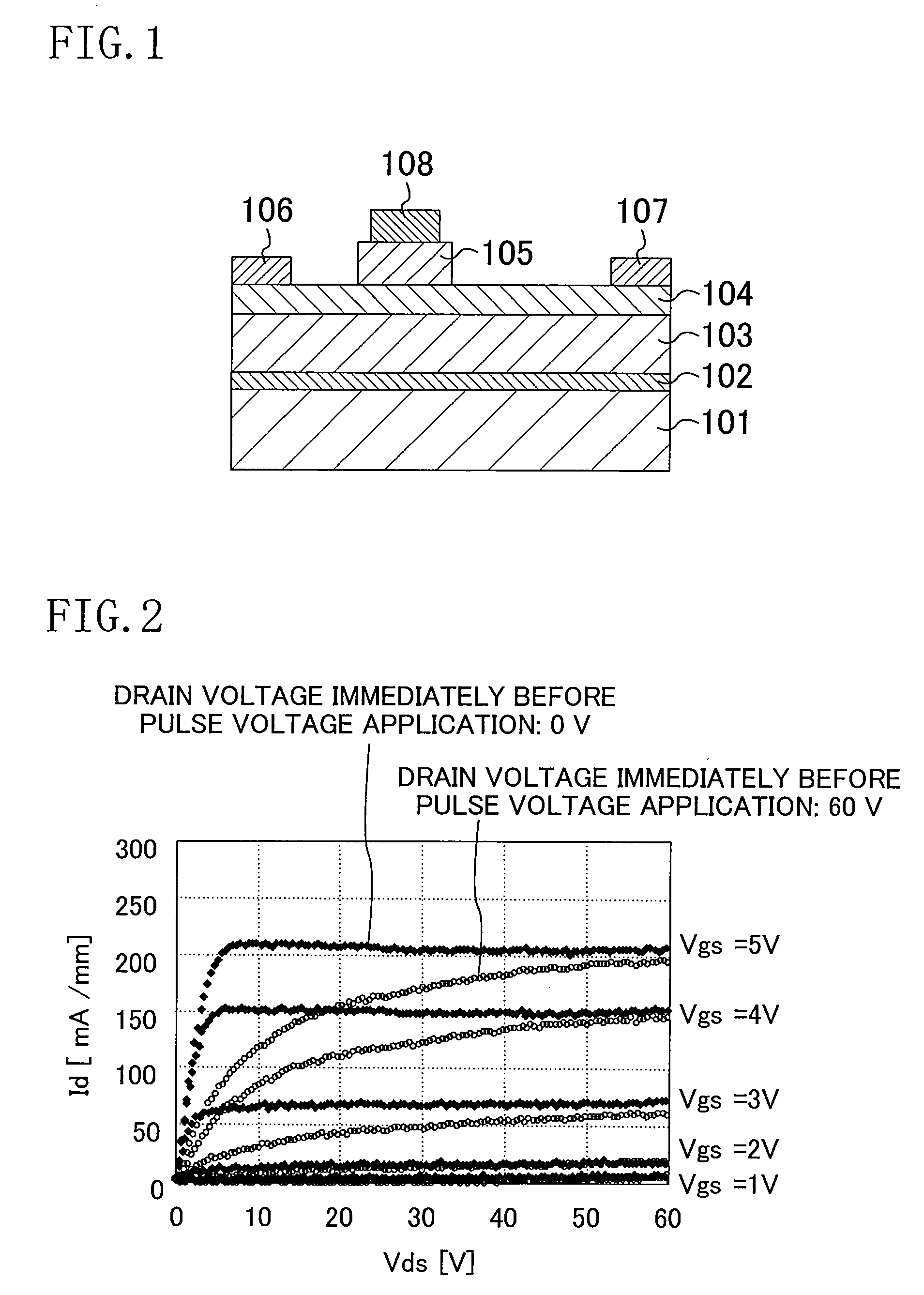
[0020]FIG. 8 is a graph showing the relation between the drain voltage (Vds) and the drain current (Id) in applying a
pulse voltage to the transistor of the second comparative example. As shown in FIG. 8, for the transistor of the second comparative example, even in the case where a high drain voltage (60 V) is applied immediately before
pulse voltage application, the transistor exhibits almost the same characteristics as those in the case of a drain voltage of 0 V immediately before
pulse voltage application. From this, it is found that the current collapse is prevented.
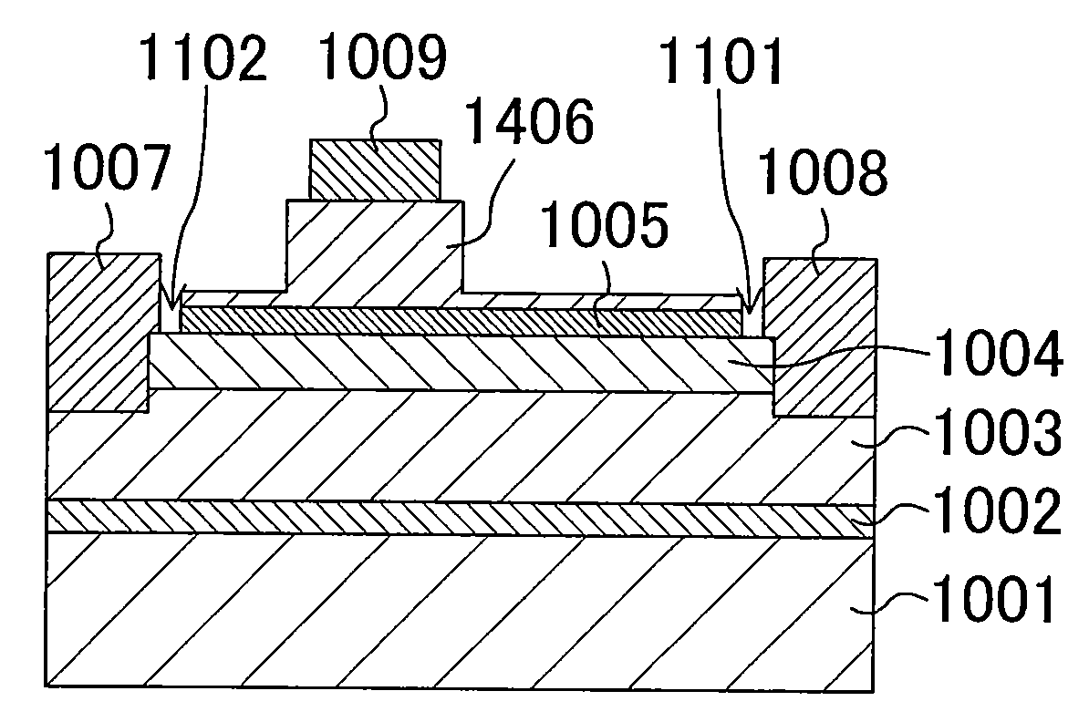
[0024]With the structure of this transistor, the first p-type semiconductor layer is formed between the second semiconductor layer and the second p-type semiconductor layer, and provided so that the first region and the second region are interposed between the layer and the drain electrode and the source electrode in order not to come into contact with the electrodes. Thus, like the transistor of the second comparative example described above, the first p-type semiconductor layer can be provided to widen the difference between the
threshold voltage Vth1 below the gate electrode and the threshold voltage Vth2 below the side of the gate electrode, so that the transistor can
resist the influence of the
surface states. This leads to prevention of the current collapse. Moreover, the first p-type semiconductor layer is provided not to come into contact with the source electrode and the drain electrode. Thus, a leakage current can be decreased as compared with the transistor of the second comparative example described above. Accordingly, with the transistor according to the present invention, a normally-off type transistor can be provided which prevents the current collapse and has a decreased leakage current.
[0026]Desirably, the first p-type semiconductor layer is made of AlxGa1-xN (0≦x≦1), the second p-type semiconductor layer is made of AlyGa1-yN (0≦y≦1), and the
layers satisfy x≧y. In this case, as in the case described above, the
lattice constant of the first p-type semiconductor layer approaches the lattice constants of the first and second semiconductor
layers, so that the first p-type semiconductor layer can be grown with
crystal defects prevented from occurring. Moreover, since the Al concentration in the second p-type semiconductor layer is lower than that of the first p-type semiconductor layer, the threshold voltage Vth1 below the gate electrode can be made higher. This is effective at providing a normally-off type transistor.
[0027]The case where the first region has a width in the
gate length direction of 0.7 to 4.5 μm inclusive is preferable because reduction of leakage current and prevention of current collapse can be conducted more effectively.
[0029]This method is characterized in that in the step (c), a portion of the first p-type semiconductor layer is removed to leave a predetermined region (a region between the first and second regions as seen from a horizontal plane), and in the step (d), the recesses for providing the source electrode and the drain electrode are formed at the sides of the first and second regions, respectively. Thereby, a groove with a bottom composed of the first region is formed between the drain electrode and the first p-type semiconductor layer, and a groove with a bottom composed of the second region is formed between the source electrode and the first p-type semiconductor layer. As a result of this, the first p-type semiconductor layer capable of reducing the influence of the
surface states can be provided on the second semiconductor layer, and the source electrode and the drain electrode can be electrically isolated from the first p-type semiconductor layer. Accordingly, with the method for fabricating a transistor according to the present invention, a normally-off type transistor can be fabricated which prevents the current collapse and has a decreased leakage current.
