

Manufacturing Method of Semiconductor Device
a manufacturing method and semiconductor technology, applied in semiconductor devices, photomechanical treatment, instruments, etc., can solve the problems of increased cost and decreased throughput, and achieve the effects of high reliability, thin film processing, and easy operation of thin films
- Summary
- Abstract
- Description
- Claims
- Application Information
AI Technical Summary
Benefits of technology
Problems solved by technology
Method used
Image

Examples
embodiment mode 1
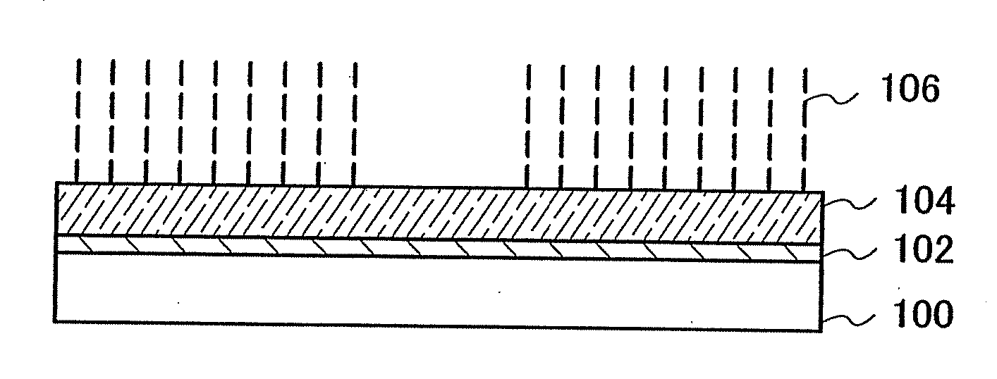
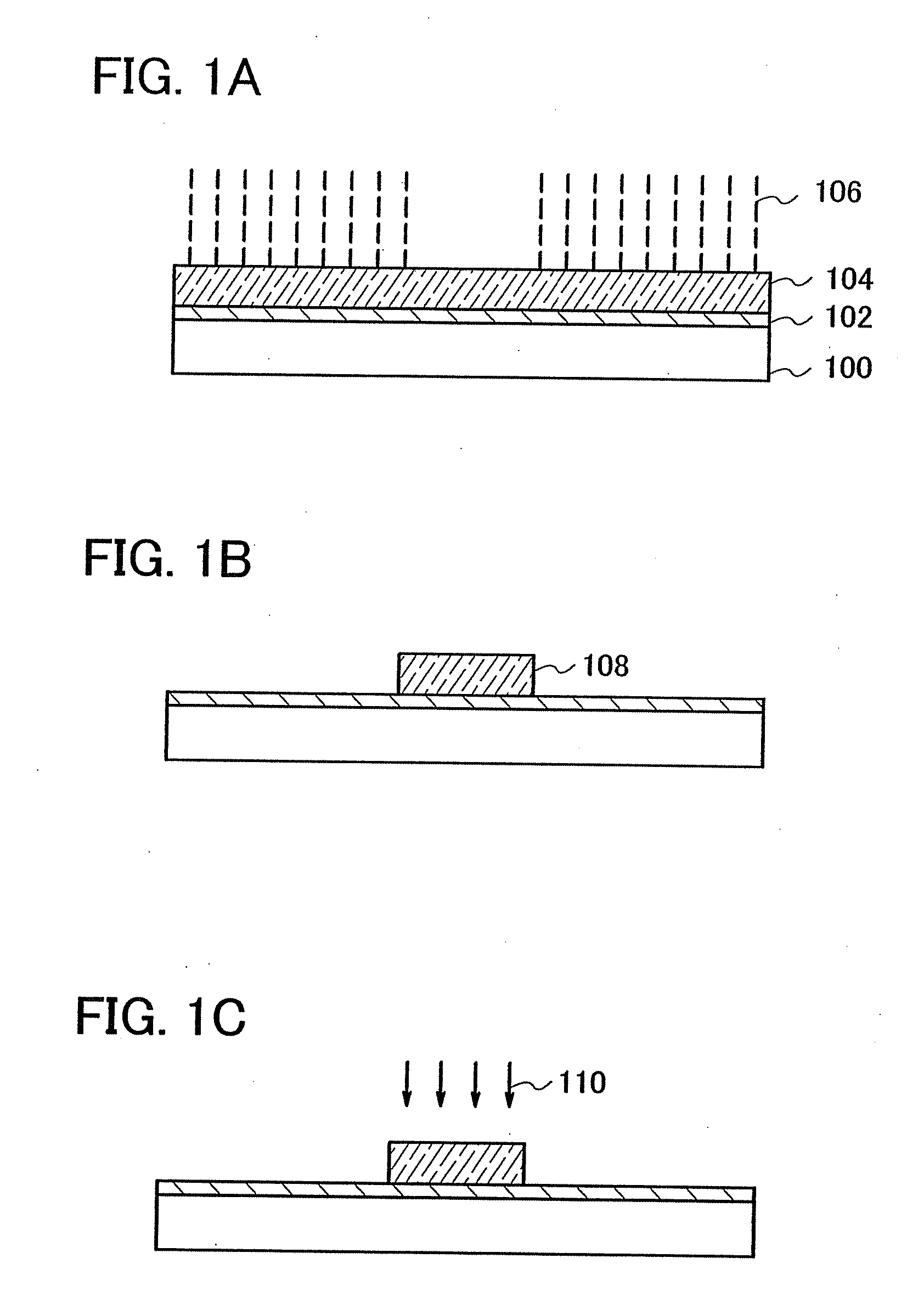
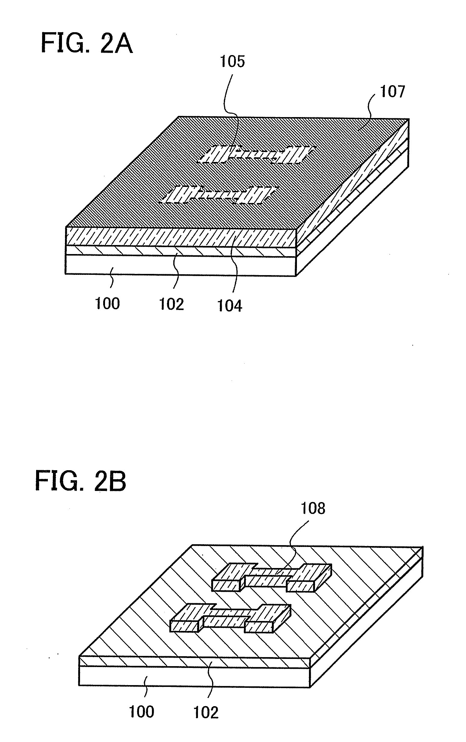
[0063]One feature of the present invention is to process a desired region without carrying out a lithography process that uses a photoresist. In Embodiment Mode 1, a thin film pattern with a desired shape is formed by irradiation with a laser beam. Hereinafter, an example of a method for forming a thin film pattern with a desired shape by processing a thin film will be specifically described with reference to FIGS. 1A to 1C. In addition, FIGS. 2A and 2B show examples of perspective views of FIGS. 1A to 1C.
[0064]Over a substrate 100, an insulating layer 102 and a light absorption layer 104 are sequentially stacked. The light absorption layer 104 is selectively irradiated with a laser beam 106 (FIG. 1A, FIG. 2A). In FIG. 2A, a region of the light absorption layer 104, which is irradiated with the laser beam 106, is referred to as an irradiated region 107, and a region of the light absorption layer 104, which is not irradiated with the laser beam 106, is referred to as a non-irradiated...
embodiment mode 2
[0130]Embodiment Mode 2 will describe examples of a method for processing a thin film, which are different from those of the above embodiment mode, with reference to FIGS. 5A to 6D. Here, an example of processing a conductive layer functioning as an electrode or a wiring will be described.
[0131]An insulating layer 502, a first material layer 504, and a light absorption layer 506 are sequentially stacked over a substrate 500. The light absorption layer 506 is selectively irradiated with a laser beam 508 (FIG. 5A). Since a substrate and an insulating layer similar to the substrate 100 and the insulating layer 102 described in Embodiment Mode 1 can be used for the substrate 500 and the insulating layer 502, the explanations thereof are omitted.
[0132]The first material layer 504 is formed using a material in accordance with the purpose. For example, when a conductive layer is desired to be formed as the first material layer 504, a conductive material such as a metal element of tantalum ...
embodiment mode 3
[0153]Embodiment Mode 3 will describe examples of a method for processing a thin film, which are different from those of the above embodiment modes, with reference to FIGS. 3A to 4D. Here, an example in which a thin film is processed to form an opening for electrically connecting a conductive layer with another conductive layer, or for electrically connecting a conductive layer with a semiconductor layer, will be described.
[0154]An insulating layer 302, a light absorption layer 304, and a light-transmitting layer 306 are sequentially stacked over a substrate 300. The light absorption layer 304 is selectively irradiated with a laser beam 308 from the light-transmitting layer 306 side (FIG. 3A). Since a substrate and an insulating layer similar to the substrate 100 and the insulating layer 102 described in Embodiment Mode 1 can be used for the substrate 300 and the insulating layer 302, the explanations thereof are omitted.
[0155]A layer that absorbs the laser beam 308 is formed as the...
PUM
| Property | Measurement | Unit |
|---|---|---|
| thickness | aaaaa | aaaaa |
| tensile stress | aaaaa | aaaaa |
| thickness | aaaaa | aaaaa |
Abstract
Description
Claims
Application Information