Evaluation Method for Crystal Defect in Silicon Single Crystal Wafer

a single crystal wafer and crystal defect technology, applied in the testing/measurement of individual semiconductor devices, semiconductor/solid-state devices, instruments, etc., can solve the problems of labor and cost, small crystal defects, and inability to detect such crystal defects by examination, so as to reduce labor and cost, the effect of small void defects

Inactive Publication Date: 2008-06-26
SHIN-ETSU HANDOTAI CO LTD
View PDF2 Cites 7 Cited by
  • Summary
  • Abstract
  • Description
  • Claims
  • Application Information

AI Technical Summary

Benefits of technology

[0021]When scanning is carried out while irradiating the main surface of the silicon single crystal wafer with the laser beam at fixed intervals, an entire region of the wafer in a radial direction can be evaluated in a shorter time.
[0022]As explained above, according to the present invention, since small void defects including DSODs in the silicon single crystal wafer are evaluated based on the infrared laser scattering tomograph without using the Cu deposition method, the small void defects can be simply and further precisely evaluated without requiring a wasteful cost.

Problems solved by technology

However, it has been revealed that very small crystal defects are present even in a silicon single crystal subjected to crystal growth in a neutral region to suppress such crystal defects.
Since such a crystal defect has a very small defect size (a diameter: approximately 15 nm to 20 nm), a particle counter used for regular crystal examination cannot detect such crystal defects.
However, when the wafer is rejected on this stage, wafer machining is performed even with respect to a rejected lot without exception, and the rejected product takes labor and cost like a conforming product but is finally discarded, which is hence wasteful.
Furthermore, the defect is hard to be discriminated from, e.g., a scratch caused by machining, and hence there is a problem in a measurement precision.
This small void defect may also affect characteristics of an integrated circuit formed on the surface layer of the silicon single crystal wafer in some cases.

Method used


Image

  • Evaluation Method for Crystal Defect in Silicon Single Crystal Wafer
  • Evaluation Method for Crystal Defect in Silicon Single Crystal Wafer
  • Evaluation Method for Crystal Defect in Silicon Single Crystal Wafer

Examples


experiment 1

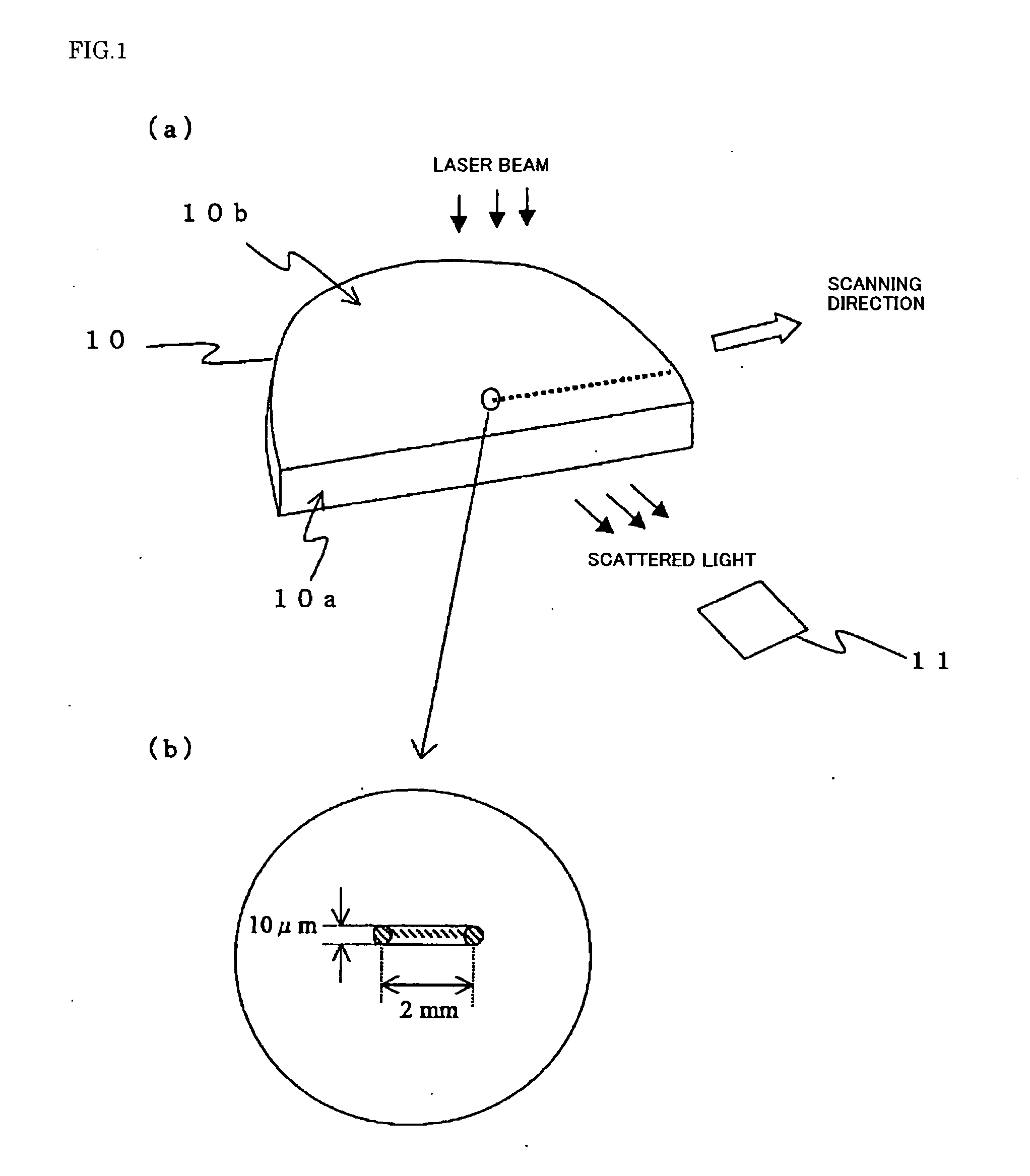
[0045]An example of examining a relationship between crystal defects detected by the infrared laser scattering tomograph method according to the present invention and crystal defects detected by the conventional Cu deposition method will be described.

[0046]First, a silicon single crystal having a diameter 300 mm and a crystal orientation 100> was pulled upwardly by the CZ method. As crystal growth conditions, and a growth rate was selected in such a manner that DSODs alone are present without an FPD, thereby producing a single crystal.

[0047]After silicon single crystal growth, the grown silicon single crystal was ground by a cylindrical grinder to remove a cone part and a tail part of the single crystal, and then a crystal fixed-diameter part was cut into a length of approximately 25 cm to provide a single crystal block.

[0048]A wafer of approximately 1 mm was sliced from the cone side of this single crystal block by a slicer, a surface of this wafer was ground approximately 300 μm b...

experiment 2

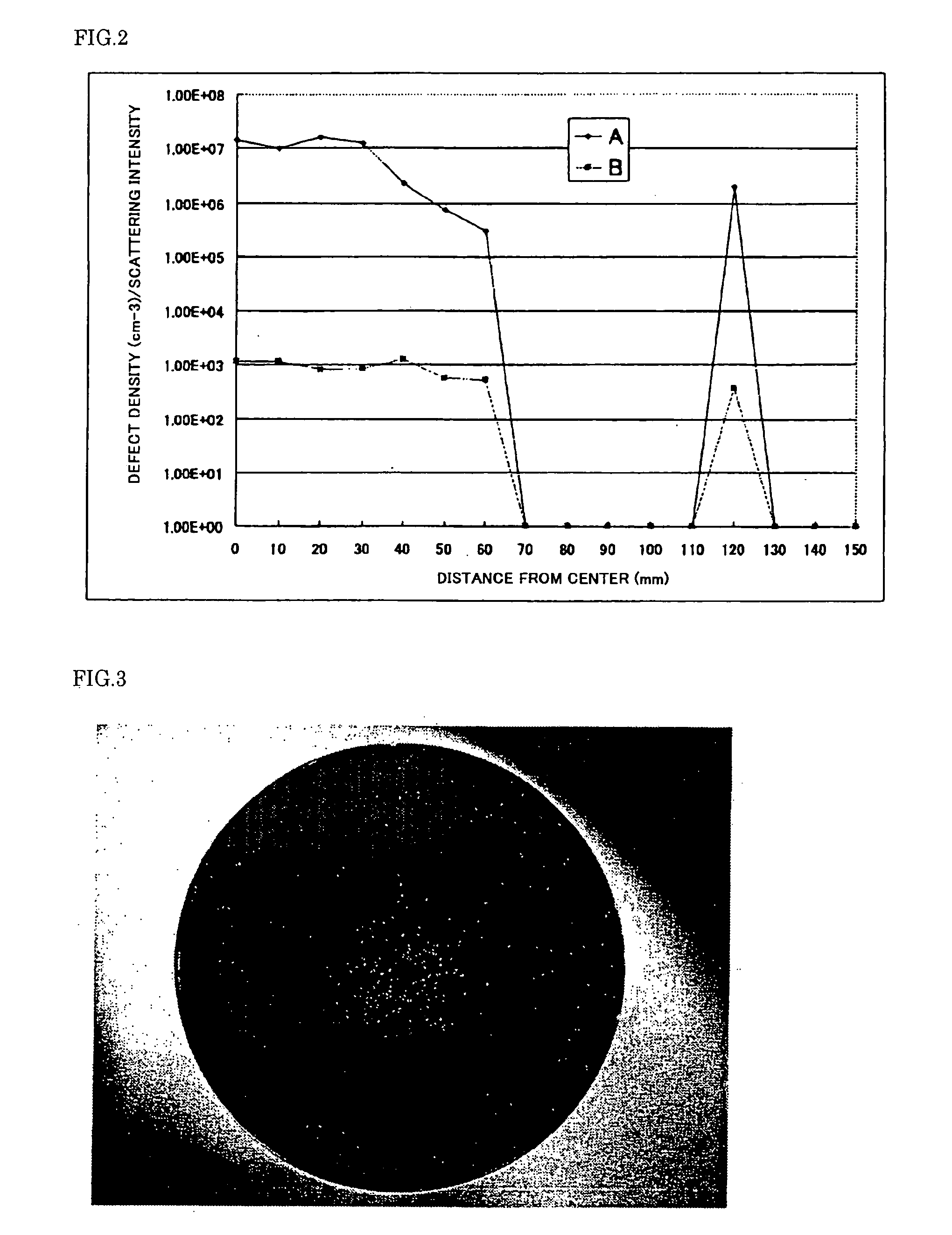
[0057]Another example of examining a relationship between crystal defects detected by the infrared laser scattering tomograph method according to the present invention and crystal defects detected by the conventional Cu deposition method will now be explained.

[0058]Like Experiment 1, two single crystal blocks (A, B) were cut from a silicon single crystal having a diameter 300 mm and a crystal orientation 100> pulled by the CZ method, and silicon single crystal wafers were sliced from the single crystal blocks (A, B).

[0059]Moreover, like Experiment 1, a silicon single crystal wafer for evaluation was made, and evaluation of crystal defects based on the infrared laser scattering tomograph method and evaluation of crystal defects based on the Cu deposition method were carried out.

[0060]FIG. 4 shows its result. Here, horizontal axis in FIG. 4 represents a distance from the wafer center, and vertical axis represents a defect density and a scattering intensity.

[0061]In FIG. 4, a line grap...


PUM


Abstract

The present invention provides an evaluation method for a crystal defect in a silicon single crystal wafer based on an infrared laser scattering tomograph method, wherein at least, the silicon single crystal wafer is irradiated with a laser beam, and light that enters the silicon single crystal wafer is scattered by a crystal defect, and the scattered light is detected to evaluate a Direct Surface Oxide Defect (DSOD) and a void defect smaller than the DSOD in the silicon single crystal wafer. As a result, the evaluation method for a crystal defect in a silicon single crystal wafer that can simply and precisely evaluate, e.g., a small DSOD, which can be conventionally evaluated based on a Cu deposition method alone, without requiring a wasteful cost.

Description

TECHNICAL FIELD[0001]The present invention relates to an evaluation method for a crystal defect in a silicon single crystal wafer that serves as a substrate for manufacturing, e.g., a semiconductor integrated circuit.BACKGROUND ART[0002]Silicon single crystal wafers are used mostly as materials forming a semiconductor integrated circuit. Various kinds of stresses are applied to a wafer by a heat treatment or machining until a semiconductor device is formed on a surface layer of a silicon single crystal wafer to provide an integrated circuit. Therefore, a silicon single crystal wafer produced from a silicon single crystal obtained by a Czochralski method (which will be referred to as a CZ method hereinafter) is superior in strength, and hence this wafer tends to be often used.[0003]However, in recent years, with density growth of an integration degree of a semiconductor integrated circuit and attendant miniaturization of a device circuit, a quality requirement for a silicon single cr...

Claims


Application Information

Patent Timeline
Patent Type & Authority Applications(United States)
IPC IPC(8): H01L21/66
CPCG01N21/47G01N21/896G01N21/9501G01N21/9505H01L22/24G01N2021/4735G01N2021/8477G01N2021/8965G01N2021/4707H01L22/00
Inventor SAITO, HISAYUKIKITAGAWARA, YUTAKA
Owner SHIN-ETSU HANDOTAI CO LTD
Why Eureka
Try Eureka