Bonding method and bonding material using metal particle

a metal particle and bonding method technology, applied in the field of bonding materials, can solve the problems of insufficient heat dissipation and bonding reliability of a method for achieving metallic bonding at an interface, no material to replace high-temperature solder, and difficult to completely remove the protective film

Inactive Publication Date: 2008-07-03
HITACHI LTD
View PDF11 Cites 74 Cited by
  • Summary
  • Abstract
  • Description
  • Claims
  • Application Information

AI Technical Summary

Benefits of technology

[0012]It has been found that addition of a reducing agent composed of an organic substance to a metal particle precursor being at least one selected from the group consisting of a particle of a metal oxide, a particle of silver carbonate, and a particle of silver acetate and having an average particle diameter of not less than 1 nm and not more than 50 μm causes the metal particle precursor to be reduced at a lower temperature than when the metal particle precursor alone is thermally decomposed to produce a metal particle having an average particle diameter of not more than 100 nm. It has also been found at this time that application of pressure between members to be bonded using a bonding material containing more than 50 parts by mass and not more than 99 parts by mass of a metal particle precursor being at least one selected from the group consisting of a particle of a metal oxide, a particle of a metal carbonate, and a particle of a metal carboxylate and having an average particle diameter of not less than 1 nm and not more than 50 μm per 100 parts by mass of the bonding material makes it possible to acquire a closer sintered silver than that using a bonding material containing only not more than 50 parts by mass of the metal particle precursor and achieve metallic bonding at a bonding interface.
[0015]According to the present invention, it is possible to provide a bonding material and a bonding method capable of realizing bonding by metallic bonding at a bonding interface at a lower temperature compared to a bonding material using a metal particle having an average particle diameter of not more than 100 nm.

Problems solved by technology

However, since a method using such a conductive adhesive uses a binder as a bonding mechanism at an interface, it is inferior in heat dissipation and bonding reliability to a method for achieving metallic bonding at an interface.
Although solder is under pressure to be lead-free, there is as yet no material to replace high-temperature solder.
Although the protective film of the organic substance needs to be removed at the time of bonding, it is difficult to completely remove the protective film by heating at a low temperature, and sufficient bonding strength is hard to achieve.
If a protective film made of an organic substance for metal particles is molecularly designed to decompose at a low temperature, metal particles produced at a room temperature of 20 to 30° C. immediately cohere, and thus it is difficult to produce metal particles which can sinter at a low temperature.
In addition, since production of metal particles having an average particle diameter of 100 nm or less involves troublesome work such as removal of impurities after the production, reducing the cost of a bonding material is difficult.
As described above, a bonding method using metal particles having an average particle diameter of 100 nm or less has practical problems remaining to be solved such as production of metal particles, removal of impurities from and storage of metal particles after production, and handling of metal particles.
However, the volume of tertiary fatty acid silver salt, which is a precursor of a silver nanoparticle, shrinks, the content of silver in the tertiary fatty acid silver salt is not high, and the volatilization temperature of an organic substance generated when the tertiary fatty acid silver salt decomposes is not low.
Accordingly, it is difficult to use more than 50 parts by mass of the silver nanoparticle precursor per 100 parts by mass of the conductive composition in a bonding material.
Additionally, since a heating time of 10 minutes or more is required, shortening of process time is difficult.
Moreover, since adhesion is achieved mainly by using a binder at an interface, as in Patent Document 1, it is difficult to acquire a close sintered silver layer and achieve metallic bonding at an interface after bonding.

Method used


Image

  • Bonding method and bonding material using metal particle
  • Bonding method and bonding material using metal particle
  • Bonding method and bonding material using metal particle

Examples


example 1

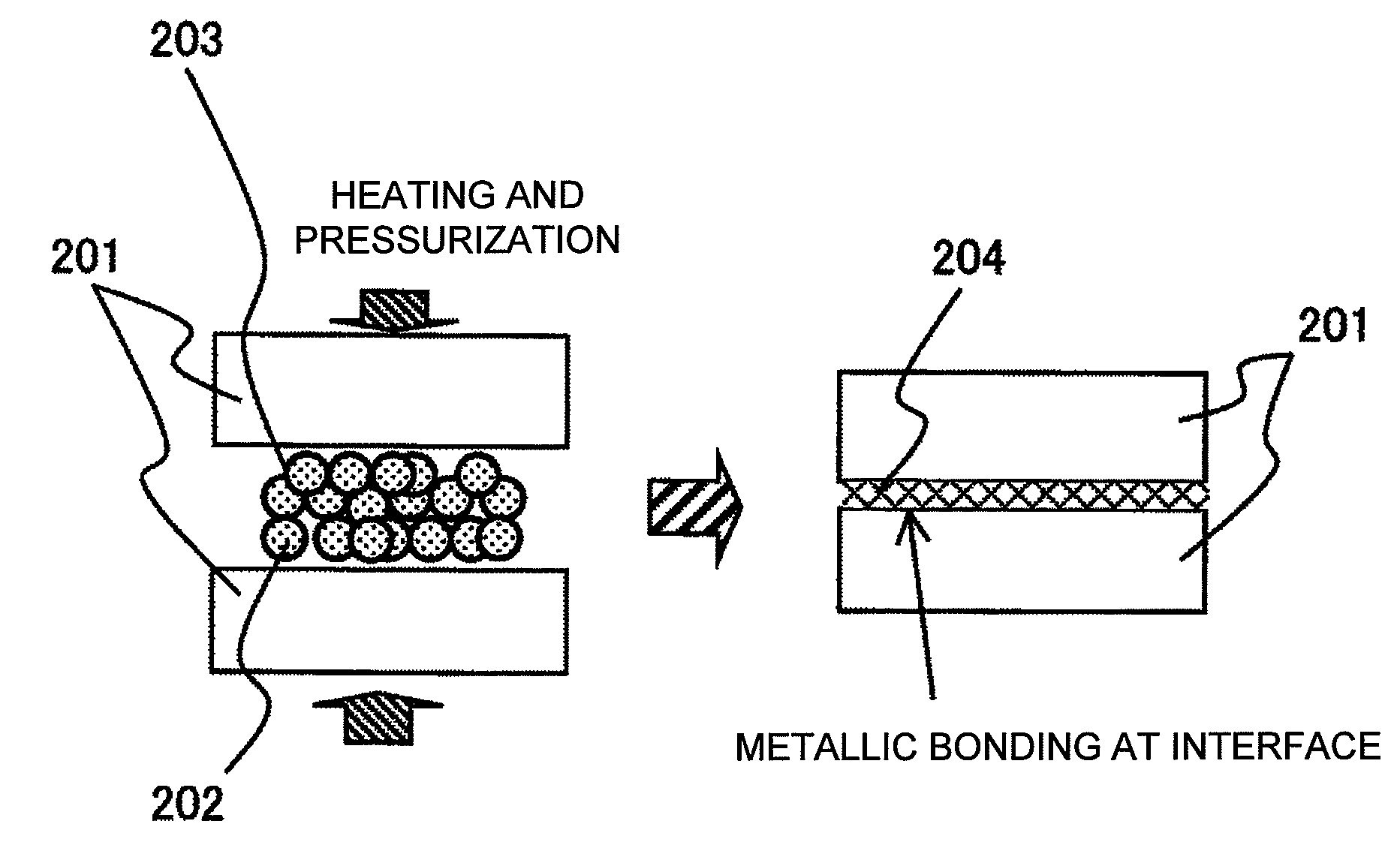
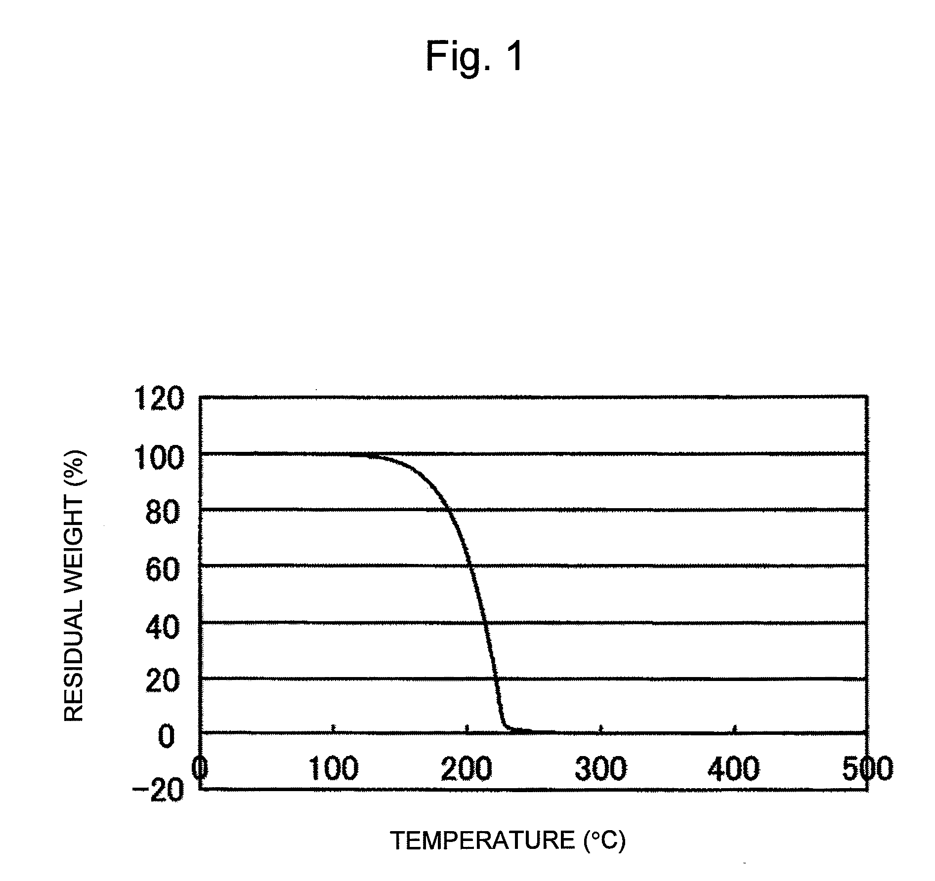
[0079]In Example 1, silver oxide (Ag2O) particles having an average particle diameter of about 2 μm were used, and myristyl alcohol (made by Wako Pure Chemical Industries, Ltd.) was used as an organic substance serving as a reducing agent. FIG. 1 shows the result of thermogravimetric measurement of myristyl alcohol. The thermogravimetric measurement was performed using a TG / DTA6200 made by Seiko Instruments Inc. At this time, the measurement was performed at a rate of temperature rise of 10° C. / min in the atmosphere. The result shows that the rate of weight loss versus temperature of myristyl alcohol at 244° C. was 99% or more. Myristyl alcohol and silver oxide (Ag2O) particles were then mixed such that the mixing ratio was 1:4 by weight. Actually, a bonding material was produced using 0.8 g of silver oxide (Ag2O) and 0.2 g of myristyl alcohol. Since myristyl alcohol is solid at room temperature, the myristyl alcohol was mixed with particles of the silver oxide (Ag2O) for 10 minutes...

example 2

[0085]In Example 2, bonding was performed using each of a bonding material (bonding material ) formed by mixing silver carbonate particles (made by Wako Pure Chemical Industries, Ltd.) having an average particle diameter of about 1 μm and myristyl alcohol in the weight ratio of 4:1, a bonding material (bonding material ) formed by mixing silver acetate particles (made by Wako Pure Chemical Industries, Ltd.) and myristyl alcohol in the weight ratio of 4:1, and a bonding material (bonding material ) formed by mixing silver oxide particles having an average particle diameter of about 2 μm and silver acetate particles (made by Wako Pure Chemical Industries, Ltd.) in the weight ratio of 4:1, and shear strength measurement was performed. Each pair of components was mixed using a mortar. Of test pieces for bonding, the upper one was 5 mm in diameter and was 2 mm in thickness while the lower one was 10 mm in diameter and was 5 mm in thickness. The front surface of the lower test piece was p...

example 3

[0091]FIGS. 6(A) and 6(B) are views showing the structure of a non-insulated semiconductor apparatus serving as an example of the present invention. FIG. 6(A) is a top view, and FIG. 6(B) is a sectional view of FIG. 6(A) taken along line A-A′. Semiconductor devices (MOSFET) 301 are mounted on a ceramic insulating substrate 302, and the ceramic insulating substrate 302 is mounted on a base material 303. After that, an epoxy resin case 304, bonding wires 305, and an epoxy resin lid 306 are provided, and the epoxy resin case 304 is filled with silicone gel resin 307. The ceramic insulating substrate 302 on the base material 303 is bonded through a bonding layer 308 composed of a paste material formed by dispersing silver oxide (Ag2O) particles having an average particle diameter of about 2 μm and myristyl alcohol in the weight ratio of 4:1 in a toluene solution. Eight MOSFET devices 301 made of Si are bonded to copper plates 302a of the ceramic insulating substrate 302 through bonding ...


PUM

PropertyMeasurementUnit
particle diameteraaaaaaaaaa

Abstract

It is an object of this invention to provide a bonding material capable of realizing bonding by metallic bonding at a bonding interface at a lower temperature compared to a bonding material using a metal particle having an average particle diameter of not more than 100 nm and a bonding method. There is provided a bonding material including a metal particle precursor being at least one selected from the group consisting of a particle of a metal oxide, a particle of a metal carbonate, and a particle of a metal carboxylate and having an average particle diameter of 1 nm to 50 μm and a reducing agent composed of an organic substance, wherein the content of the metal particle precursor is more than 50 parts by mass and not more than 99 parts by mass per 100 parts by mass of the bonding material.

Description

BACKGROUND OF THE INVENTION[0001]1. Field of the Invention[0002]The present invention relates to a bonding material in a semiconductor module and a method for manufacturing the bonding material.[0003]2. Background Art[0004]In a non-insulated semiconductor apparatus which is one of power semiconductor apparatuses used in an inverter or the like, a member which fixes a semiconductor device also serves as an electrode of the semiconductor apparatus. For example, in a semiconductor apparatus in which a power transistor is mounted on a fixed member using a Sn—Pb soldering material, the fixed member (base material) serves as a collector electrode of the power transistor. When the semiconductor apparatus is in operation, a current of several amperes or more flows through the collector electrode portion, and the transistor chip generates heat. To avoid destabilization of characteristics and reduction in lifetime caused by the heat generation, the heat dissipation and long-term reliability (...

Claims


Application Information

Patent Timeline
Patent Type & Authority Applications(United States)
IPC IPC(8): B23K35/34
CPCB23K35/34B23K35/3612H01L23/3107H01L24/27H01L24/29H01L24/30H01L24/32H01L24/33H01L24/45H01L24/83H01L25/072H01L2224/04026H01L2224/05639H01L2224/2731H01L2224/29294H01L2224/29387H01L2224/29393H01L2224/30181H01L2224/32175H01L2224/33181H01L2224/45015H01L2224/45124H01L2224/73265H01L2224/83191H01L2224/83192H01L2224/83203H01L2224/83444H01L2224/83447H01L2224/8384H01L2224/83986H01L2224/85205H01L2924/01013H01L2924/01029H01L2924/0103H01L2924/01047H01L2924/01049H01L2924/0105H01L2924/01073H01L2924/01079H01L2924/01082H01L2924/0541H01L2924/09701H01L2924/10253H01L2924/13091H01L2924/16195H01L2924/19041H01L2924/19043H01L2924/19105H01L2924/19107H01L2224/2919H01L2224/32225H01L2224/32245H01L2924/01005H01L2924/01006H01L2924/01019H01L2924/01024H01L2924/01033H01L2924/01044H01L2924/01045H01L2924/01074H01L2924/01076H01L2924/01077H01L2924/01078H01L2924/014H01L2924/0665H01L2224/29101H01L2224/83455H01L2924/0132H01L2224/8584H01L2224/45147H01L2924/15747H01L2224/48227H01L2224/48247H01L2224/29111H01L2224/48739H01L2224/29139H01L2924/01014H01L2924/01028H01L2924/12041H01L2924/00014H01L2924/2076H01L2924/00H01L2924/00012H01L2924/3512H01L2924/00011H01L2924/15787H01L2224/48839H01L24/73H01L2924/181H01L2224/83205H01L2224/48
Inventor YASUDA, YUSUKEMORITA, TOSHIAKIIDE, EIICHIHOZOJI, HIROSHIISHII, TOSHIAKI
Owner HITACHI LTD
Why Eureka
Try Eureka