OLED with protective electrode

Active Publication Date: 2008-07-03
GLOBAL OLED TECH
View PDF18 Cites 21 Cited by
  • Summary
  • Abstract
  • Description
  • Claims
  • Application Information

AI Technical Summary

Benefits of technology

[0025]The present invention provides an OLED device having

Problems solved by technology

However, the materials comprising the organic EL element are sensitive and, in particular, are easily destroyed by moisture and high temperatures (for example greater than 140 degrees C.).
It has been found that one of the key factors that limits the efficiency of OLED devices is the inefficiency in extracting the photons generated by the electron-hole recombination out of the OLED devices.
Due to the relatively high optical indices of the organic and transparent electrode materials used, most of the photons generated by the recombination process are actually trapped in the devices due to total internal reflection.
In general, up to 80% of the light may be lost in this manner.
Moreover, the organic and electrode materials absorb light, further reducing the device efficiency.
Such electrodes suffer from a variety of handicaps, principally inadequate conductivity and, in some circumstances, transparency.
In top-emitting device structures, such sputter-deposited layers may also physically damage the underlying organic material layers.
However, the described barrier layers and sputter deposited electrode layers typically are not sufficiently impermeable to environmental contaminants when employed as the transparent top e

Method used


Image

  • OLED with protective electrode
  • OLED with protective electrode
  • OLED with protective electrode

Examples


Embodiment Construction

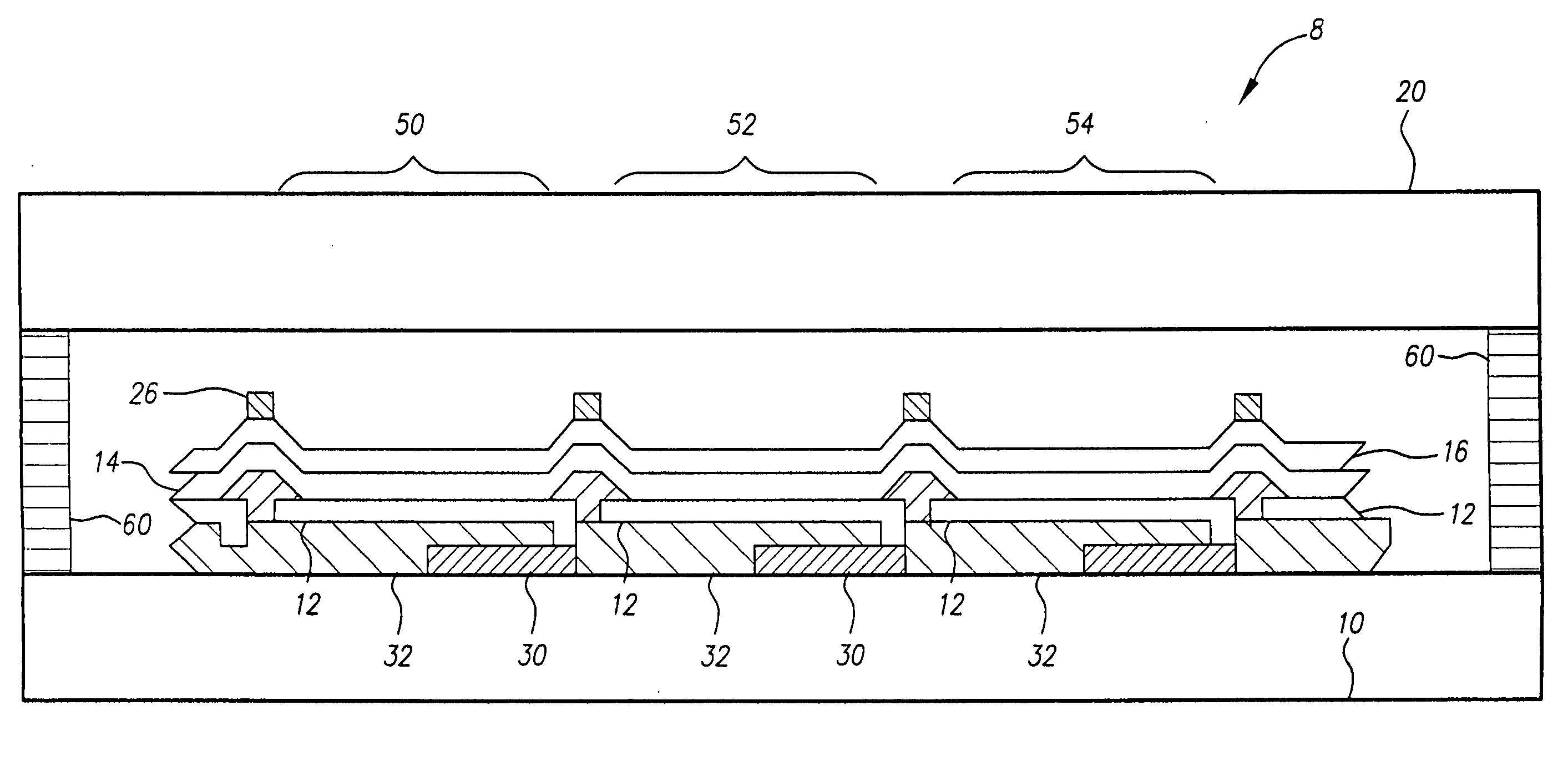
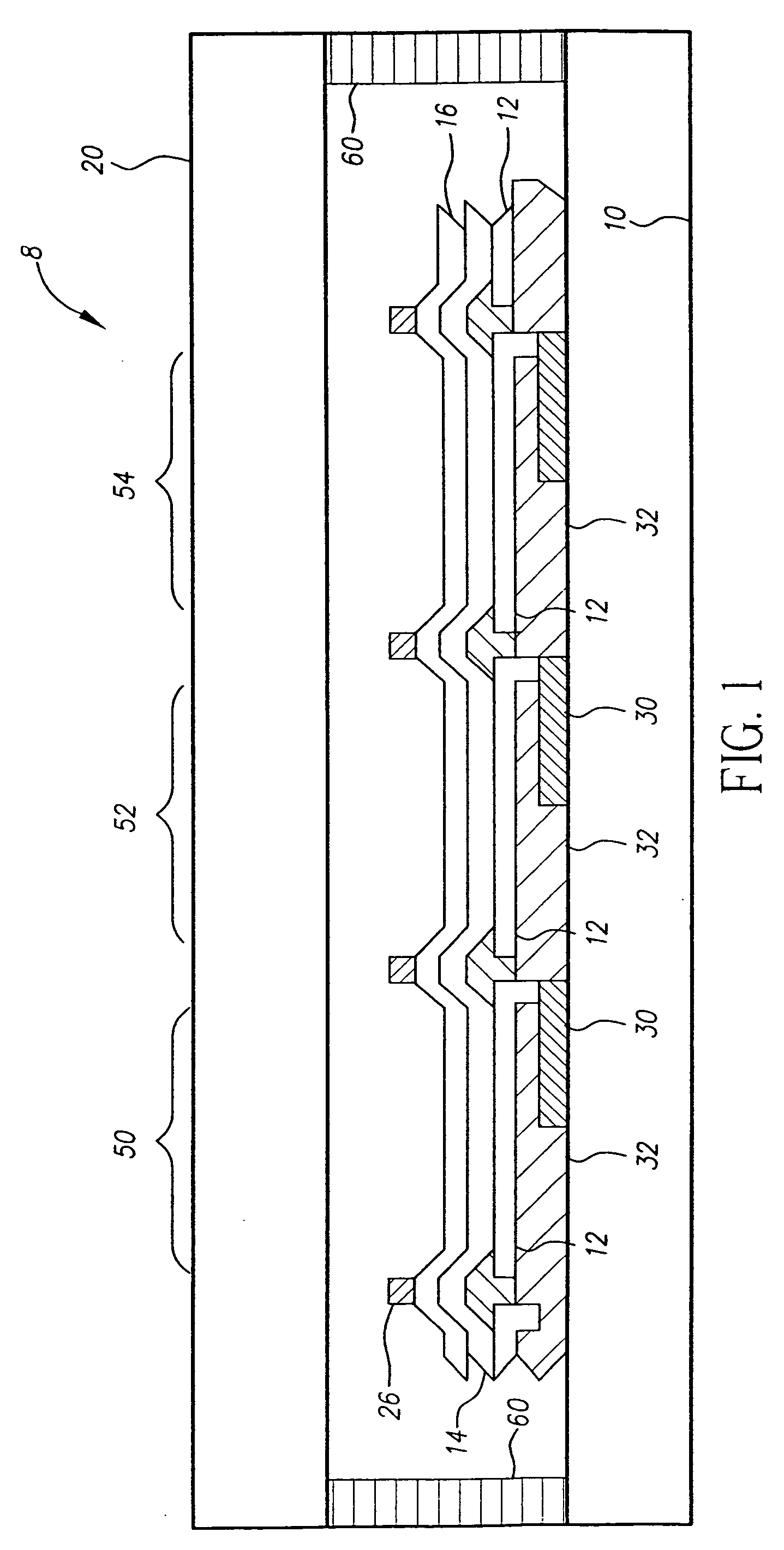
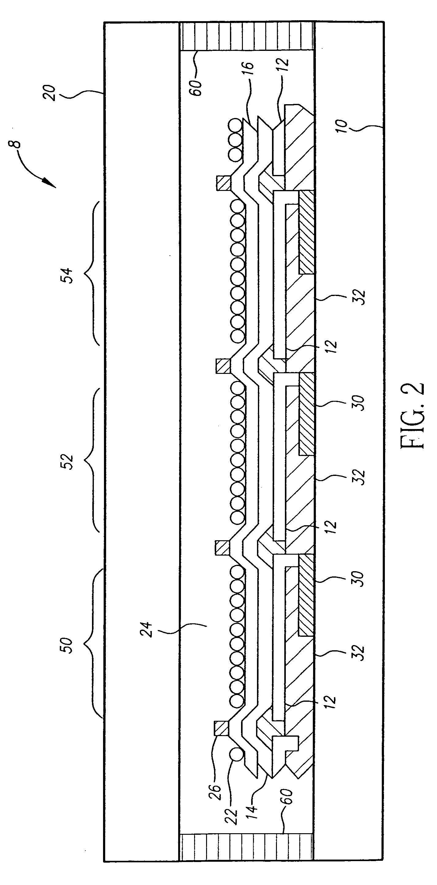
[0033]Referring to FIG. 1, an OLED device 8 according to one embodiment of the present invention comprises a substrate 10, a first electrode 12, a conductive protective electrode 16 comprising a transparent conductive oxide wherein the conductive protective electrode 16 is a hermetic layer having a thickness less than 100 nm, and one or more organic layers 14 formed between the first electrode 12 and the conductive protective electrode 16, at least one organic layer being a light-emitting layer; and a patterned auxiliary electrode 26 in electrical contact with the conductive protective electrode 16.

[0034]In a top-emitter embodiment of the present invention, the conductive protective electrode 16 is a transparent top electrode and the first electrode 12 is a bottom electrode. The bottom electrode may be reflective. It is preferred that the conductive protective electrode 16 have a refractive optical index equal to or greater than the refractive optical index of the one or more organi...


PUM


Abstract

An OLED device, comprising: a first electrode; a conductive protective electrode comprising a transparent conductive oxide layer wherein the conductive protective electrode is a hermetic layer having a thickness less than 100 nm; one or more organic layers formed between the first electrode and conductive protective electrode, at least one organic layer being a light-emitting layer; and a patterned auxiliary electrode in electrical contact with the conductive protective electrode.

Description

FIELD OF THE INVENTION[0001]The present invention relates to organic light-emitting diode (OLED) devices, and more particularly, to OLED device structures for improving light output and lifetime formed by the deposition of thin-film materials, employing a process for forming a conductive protective electrode by vapor deposition.BACKGROUND OF THE INVENTION[0002]Organic light-emitting diodes (OLEDs) are a promising technology for flat-panel displays and area illumination lamps. The technology relies upon thin-film layers of organic materials coated upon a substrate. OLED devices generally can have two formats known as small-molecule devices such as disclosed in U.S. Pat. No. 4,476,292 and polymer OLED devices such as disclosed in U.S. Pat. No. 5,247,190. Either type of OLED device may include, in sequence, an anode, an organic EL element, and a cathode. The organic EL element disposed between the anode and the cathode commonly includes an organic hole-transporting layer (HTL), an emis...

Claims


Application Information

Patent Timeline
IPC IPC(8): H01J1/62H01J9/00
CPCH01L21/3141H01L51/5203H01L51/5206H05B33/26H01L51/5262H01L51/5268H01L51/5237H10K50/805H10K50/814H10K50/841H10K50/85H10K50/854H10K50/844H01L21/0228
Inventor COK, RONALD S.
Owner GLOBAL OLED TECH
Why Eureka
Try Eureka