Nanostructured Working Electrode of an Electrochemical Sensor, Method of Manufacturing Thereof and Sensor Containing This Working Electrode

a working electrode and nanostructure technology, applied in the field of nanostructured working electrodes of electrochemical sensors, can solve the problems of material can influence the detection properties, and disadvantageous porousness and complexity of the surface structure of the printed layer

Inactive Publication Date: 2008-07-17
BVT TECH +1
View PDF9 Cites 4 Cited by
  • Summary
  • Abstract
  • Description
  • Claims
  • Application Information

AI Technical Summary

Benefits of technology

[0025]If the preparation of active layers of the sensor from the materials such as osmium, iridium, rhodium, glassy metals or other is required, it is impossible, either for physico-chemical or for chemical reasons, to transfer these materials into the form of a paste and apply them by printing. On

Problems solved by technology

The disadvantage of this method is not only the porousness and the complexity of the surface structure of the printed layer, but also the fact that the carrier material can strongly influence the detection properties of the electrode.
However, in many applications the porousness and the complexity of the surface structure of the printed layer is disadvantageous, especially when the surface of the working electrode is modified with bioactive substances such as antibodies or DNA segments.
A further disadvantage of the working electrodes with a complex surface structure is the fact that in some cases the immobilized bioch

Method used


Image

  • Nanostructured Working Electrode of an Electrochemical Sensor, Method of Manufacturing Thereof and Sensor Containing This Working Electrode
  • Nanostructured Working Electrode of an Electrochemical Sensor, Method of Manufacturing Thereof and Sensor Containing This Working Electrode
  • Nanostructured Working Electrode of an Electrochemical Sensor, Method of Manufacturing Thereof and Sensor Containing This Working Electrode

Examples


example 1

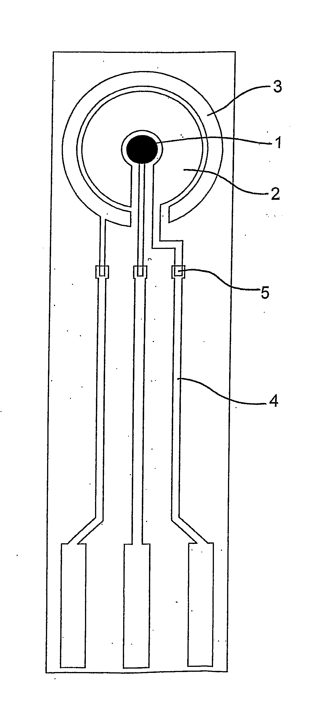
[0032]Conducting paths of silver are printed on a corundum pad by screen-printing, the pad is then left to rest for 15 minutes at the room temperature, dried for 15 to 20 minutes at 150±20° C. and subsequently fired at 850° C. In the next step, the working layer, i.e. the printed layer of the working electrode and the auxiliary electrode, is applied by screen-printing using an AuPd paste, then left to rest, dried and fired under the same conditions. The reference electrode is printed using Ag / AgCl. After resting, the motive is hardened at 150° C. for 15 min. A circle is cut with a punch from an Au film covered on both sides by protective films. The protective films are removed from the cut circle. Into the place of the working electrode, a polymeric paste is applied, the paste being the carrier medium for the cut circle. The circle is inserted into the place of the working electrode by a micromanipulator. The product is left to rest for 15 minutes and is dried for 15 to 20 minutes a...

example 2

[0033]Conducting paths of silver are printed on a corundum pad by screen-printing, the pad is then left to rest for 15 minutes at the room temperature, dried for 15 to 20 minutes at 150±20° C. and subsequently fired at 850° C. In the next step, the working layer, i.e. the printed layer of the electrode of the invention and the auxiliary electrode, is applied by screen-printing using an AuPd paste, then left to rest, dried and fired under the same conditions. The reference electrode is printed using Ag / AgCl. After resting, the motive is hardened at 150° C. for 15 min. A circle is cut with a punch from a bismuth (Bi) film. The Bi film is supplied on the mylar carrier film, the other side is protected against damage during the cutting process by a protective film. Into the place of the working electrode, a polymeric paste is applied, the paste being the carrier medium for the cut circle. The protective film is removed from the cut circle. The circle is inserted with the Bi side into th...


PUM

PropertyMeasurementUnit
Temperatureaaaaaaaaaa
Thicknessaaaaaaaaaa
Lengthaaaaaaaaaa

Abstract

A nanostructured working electrode of an electrochemical sensor wherein the working electrode is composed of a material in the form of a film and is inserted onto the sensor. The electrode can be prepared from materials the use of which was impossible in the working electrodes known in the art (e.g. metals of defined purity). A method of manufacturing of the nanostructured working electrode and an electrochemical sensor containing the nanostructured electrode is disclosed

Description

TECHNICAL FIELD[0001]The invention relates to nanostructured working electrodes of electrochemical sensors, method of manufacturing thereof and sensors containing these working electrodes.BACKGROUND ART[0002]Manufacture of electrochemical sensors by screen-printing is known (Czech patent 291411) and allows a cheap and effective manufacture of electrochemical sensors and biosensors. The principle of the manufacture of the working electrodes of such electrochemical sensors lies in applying pastes containing active materials by screen-printing. The active material (mostly gold, platinum, silver) is dispersed as very fine particles in a carrier, which ensures that the material is in the form of paste. This paste is applied to a suitable pad by means of printing. The paste is then hardened, optionally fired, which creates the active layer of the sensor, or the vehiculum of paste is evaporated and the active layer of the working electrode of the electrochemical sensor is then created by s...

Claims


Application Information

Patent Timeline
IPC IPC(8): C25B11/00B05D5/12
CPCB82Y15/00G01N27/3278G01N33/5438B82Y30/00
Inventor KREJCI, JANMALY, JANSTEJSKALOVA, RADKA
Owner BVT TECH
Why Eureka
Try Eureka