
Semiconductor package and method of manufacturing the same

Inactive Publication Date: 2008-07-17
FUJITSU LTD
View PDF1 Cites 46 Cited by
  • Summary
  • Abstract
  • Description
  • Claims
  • Application Information

AI Technical Summary

Benefits of technology

[0015]Embodiments of the present invention may solve or reduce one or more of the above-described problems.
[0020]According to the above-described semiconductor package, since carbon nanotubes have flexibility and elasticity, it is possible to repeatedly insert and extract the first conductive terminal or the second conductive terminal, so that the semiconductor device and the circuit board can be repeatedly attached to and detached from each other. As a result, it is possible to reduce the manufacturing cost of the semiconductor package by replacing only the semiconductor device or the circuit board if the semiconductor device or the circuit board is defective or fails. In particular, even if the semiconductor package contains a defective product (part or component), only the defective product may be replaced, and unlike in the conventional case, there is no need to discard good products (parts or components). Accordingly, it is possible to reduce consumption of resources. Further, since carbon nanotubes have extremely high mechanical strength, the connection mechanism can support the semiconductor device and firmly join the semiconductor device and the circuit board mechanically.
[0023]According to the above-described method, it is possible to cause carbon nanotubes to grow on the surfaces of the first conductive terminal and the second conductive terminal, and it is possible to realize a connection mechanism that allows attachment and detachment of the semiconductor device and the circuit board.

Problems solved by technology

Further, such an extra-fine pin has a disadvantage in that it can only be removed by cutting once connected by solder bonding.
However, according to these methods, when one of the multiple chips fails, it is necessary to remove all the chips.
Accordingly, these methods have a disadvantage in that not only the failed chip but also the other normal chips have to be destroyed at the time of their removal.

Method used


Image

  • Semiconductor package and method of manufacturing the same
  • Semiconductor package and method of manufacturing the same
  • Semiconductor package and method of manufacturing the same

Examples


first embodiment

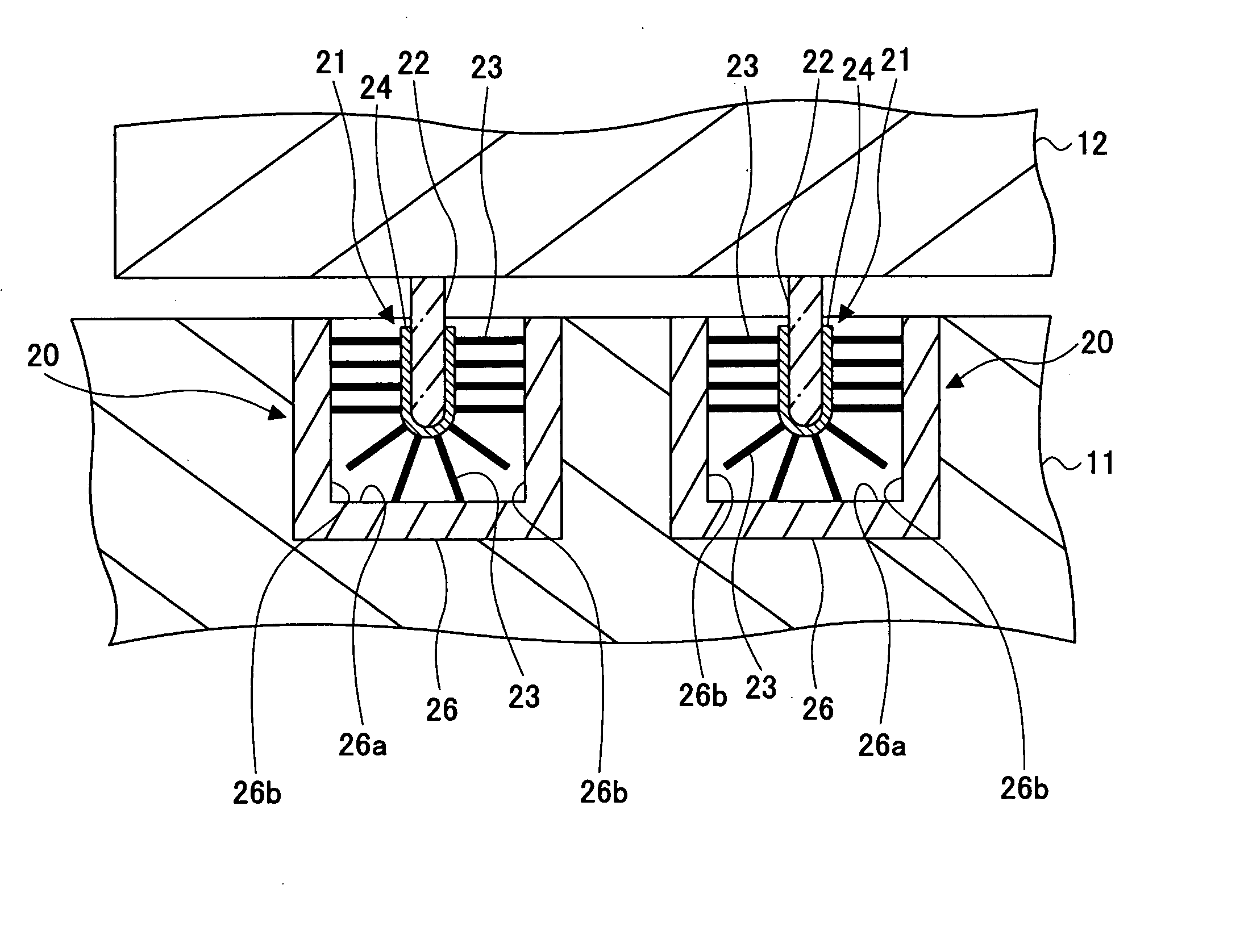
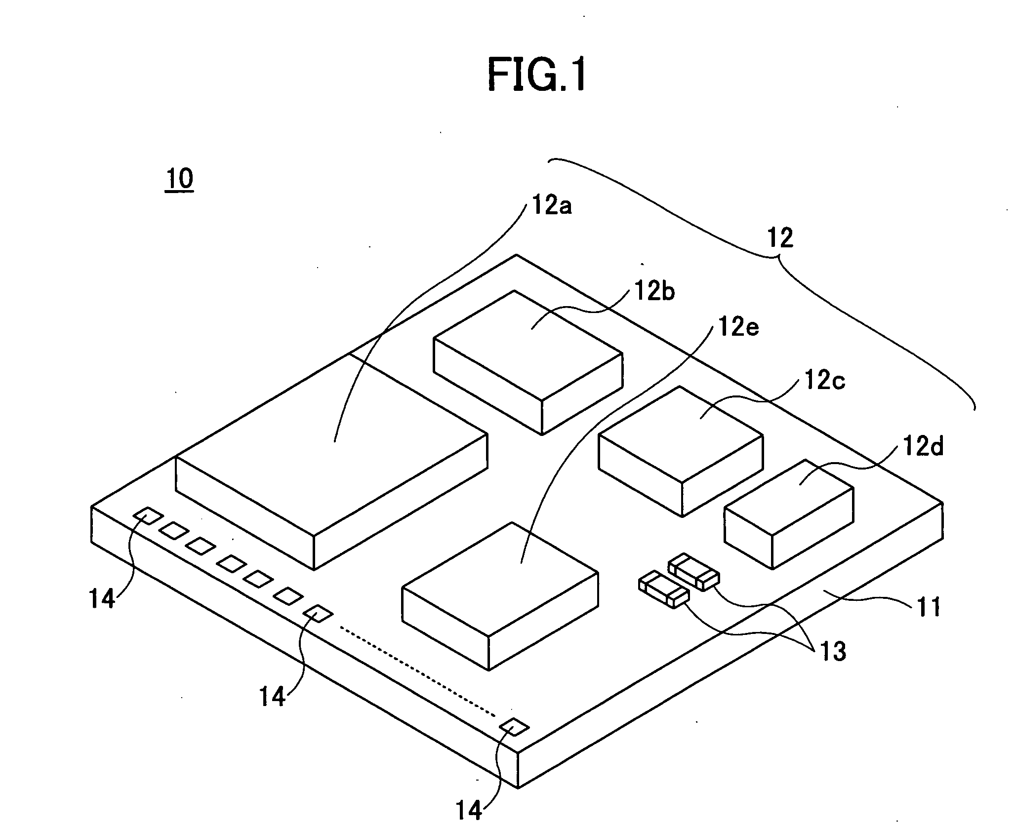
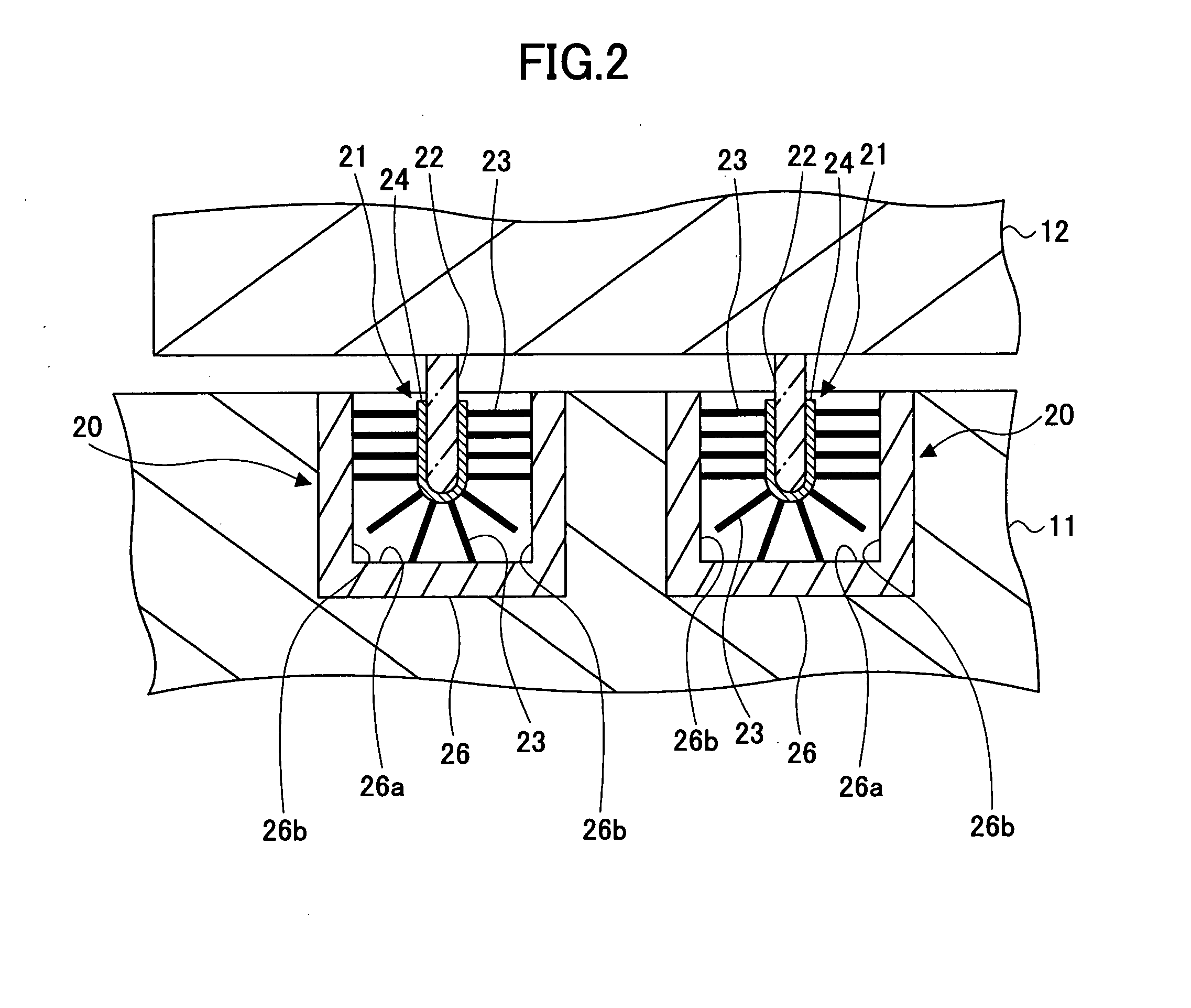
[0046]FIG. 1 is a perspective view of a semiconductor package 10 according to a first embodiment of the present invention.

[0047]Referring to FIG. 1, the semiconductor package 10 according to the first embodiment includes a circuit board 11, semiconductor devices such as an MPU (microprocessor unit) 12a, a DRAM 12b, a ROM 12c, an input / output interface IC 12d, an analog IC 12e mounted on the circuit board 11, passive elements 13 such as a resistive element and a capacitor, and external electrodes 14. Hereinafter, the MPU 12a, the DRAM 12b, the ROM 12c, the input / output interface IC 12d, and the analog IC 12e may be collectively or individually referred to as “semiconductor device 12” for convenience of description. Further, interconnects (interconnection lines) (not graphically illustrated) that electrically connect the semiconductor device 12 and the passive elements 13 are provided on the circuit board 11. The semiconductor device 12 may be, for example, a semiconductor chip or a s...

second embodiment

[0151]FIG. 17 is a schematic perspective view of a semiconductor package 110 according to a second embodiment of the present invention. FIG. 18 is a schematic exploded perspective view of the semiconductor package 110 of FIG. 17.

[0152]Referring to FIGS. 17 and 18, the semiconductor package 110 according to the second embodiment includes a chip substrate 111 on which semiconductor chips 112 are formed, a wiring (interconnection) board 121 provided on the chip substrate 111, and externally-provided semiconductor chips 125 detachably and re-attachably mounted on the wiring board 121.

[0153]The multiple semiconductor chips 112 each having various functions on a semiconductor substrate such as a silicon substrate are formed on the chip substrate 111. The semiconductor chips 112 include, for example, an MPU, memory circuits such as a DRAM and a ROM, and signal processing circuits. Chip substrate electrodes 113 for connection to the wiring board 121 are provided on the surface of each semic...


PUM


Abstract

A semiconductor package is disclosed that includes a semiconductor device; a circuit board; and a connection mechanism including a first conductive terminal provided on the semiconductor device, and a second conductive terminal provided on the circuit board side, the connection mechanism electrically connecting the semiconductor device and the circuit board via the first conductive terminal and the second conductive terminal. At least one of the first conductive terminal and the second conductive terminal of the connection mechanism includes one or more carbon nanotubes each having one end thereof fixed to the surface of the at least one of the first conductive terminal and the second conductive terminal, and extending in a direction away from the surface. The first conductive terminal and the second conductive terminal engage each other through the carbon nanotubes.

Description

CROSS-REFERENCE TO RELATED APPLICATION[0001]The present application is a continuation application filed under 35 U.S.C. 111(a) claiming benefit under 35 U.S.C. 120 and 365(c) of PCT International Application No. PCT / JP2005 / 004765, filed on Mar. 17, 2005, the entire contents of which are hereby incorporated by reference.BACKGROUND OF THE INVENTION[0002]1. Field of the Invention[0003]The present invention relates generally to semiconductor packages having an electrical connection mechanism having carbon nanotubes and methods of manufacturing the same. The present invention relates more particularly to a semiconductor package having a connection mechanism that establishes an electrical connection through the contact of carbon nanotubes with a conductor or the contact of carbon nanotubes with each other and allows repeated detachment and (re-)attachment without damage, and to a method of manufacturing the same.[0004]2. Description of the Related Art[0005]The carbon nanotube is a fine co...

Claims


Application Information

Patent Timeline
IPC IPC(8): H01L23/49H01L21/60
CPCB82Y10/00H01L2224/13582H01L24/16H01L24/90H01L2224/1134H01L2924/01004H01L2924/01013H01L2924/0102H01L2924/01022H01L2924/01027H01L2924/01029H01L2924/0103H01L2924/0104H01L2924/01042H01L2924/01046H01L2924/01073H01L2924/01074H01L2924/01075H01L2924/01078H01L2924/01079H01L2924/01082H01L2924/01327H01L2924/14H01L2924/19041H01L2924/30105H05K3/325H05K2201/026H05K2201/09472H05K2201/209H01L2224/13193H01L2924/00013H01L2924/01005H01L2924/01006H01L2924/01023H01L2924/01033H01L2924/01041H01L2924/01047H01L2924/014H01L24/12H01L2224/13693H01L2224/81141H01L2224/81385H01L2224/81899H01L2224/16237H01L2224/81191H01L2224/81193H01L2224/81345H01L2224/13099H01L2924/00014H01L2924/00011H01L2224/13563H01L2224/13078H01L2224/13541H01L24/13H01L2224/13005H01L2224/0401
Inventor AWANO, YUJIMIZUKOSHI, MASATAKA
Owner FUJITSU LTD
Learn More