Method of manufacturing semiconductor device

a manufacturing method and semiconductor technology, applied in semiconductor devices, semiconductor/solid-state device details, electrical devices, etc., can solve the problems of increasing interconnect resistance, increasing the burden on the plating step, and low uniformity of the coverage of the conductive layer, so as to suppress the burden on the plating step, and suppress the sheet resistance of the plating seed layer

Inactive Publication Date: 2008-07-24
SONY CORP
View PDF5 Cites 20 Cited by
  • Summary
  • Abstract
  • Description
  • Claims
  • Application Information

AI Technical Summary

Benefits of technology

[0014]There is a need for the present invention to provide a method for manufacturing a semiconductor device, allowing prevention of separation of a conductive layer while suppressing the burden on a plating step, and allowing enhancement in the uniformity of the coverage of the conductive layer across the substrate plane while suppressing increase in the interconnect resistance.
[0016]According to such a method for manufacturing a semiconductor device, even when the resistance of the metal other than Cu contained in the alloy layer is high, the sheet resistance of the plating seed layer is lower than that of a plating seed layer formed only of the alloy layer, because the plating seed layer arising from sequential deposition of the alloy layer and the conductive layer composed mainly of Cu is formed. Therefore, even when the concentration of the metal in the alloy layer is increased to such an extent that a continuous barrier film is formed, increase in the sheet resistance of the plating seed layer is suppressed. This eliminates the need to apply a large current in a plating step, and thus suppresses the burden on the plating step. Thus, with the burden on the plating step suppressed, a continuous barrier film can be formed at the interface between the alloy layer and the insulating film by increasing the concentration of the metal in the alloy layer. This enhances the adhesiveness between the conductive layer and the insulating film, which can prevent separation of the conductive layer. In addition, due to the low sheet resistance of the plating seed layer, unevenness of the plating growth of the conductive layer across the substrate plane is suppressed and the uniformity of the coverage of the conductive layer is enhanced. Moreover, because the alloy layer in the plating seed layer is covered by the conductive layer composed mainly of Cu, the metal on the surface side of the alloy metal is prevented from being eluted in a plating solution in the plating step. This prevents increase in the resistance of the conductive layer due to burying of the metal eluted in the plating solution in the recess together with the conductive layer at the time of filling of the recess with the conductive layer by plating.
[0017]As described above, the method for manufacturing a semiconductor device according to an embodiment of the present invention can prevent separation of a conductive layer, and thus can enhance the yield of the semiconductor device. Furthermore, the uniformity of the coverage of the conductive layer across the substrate plane is enhanced, which can suppress dishing and erosion that will occur in polishing of the conductive layer by e.g. CMP. Moreover, increase in the resistance of the conductive layer can be prevented. Consequently, when the recess is an interconnect trench and the conductive layer is an interconnect, increase in the interconnect resistance can be prevented and the interconnect reliability can be enhanced.

Problems solved by technology

However, the above-described manufacturing method involves the following problems.
This leads to the necessity for application of a large current in the plating step, and thus increases the burden on the plating step.
This causes unevenness of the plating growth of the conductive layer 18 across the plane of the substrate 11, which results in low uniformity of the coverage of the conductive layer 18.
Moreover, Mn on the surface side of the plating seed layer 17′ is easily eluted in a plating solution, which leads to a problem that the Mn eluted in the plating solution is buried in the interconnect trench 16 together with the conductive layer 18 and hence the interconnect resistance increases.

Method used


Image

  • Method of manufacturing semiconductor device
  • Method of manufacturing semiconductor device
  • Method of manufacturing semiconductor device

Examples


first embodiment

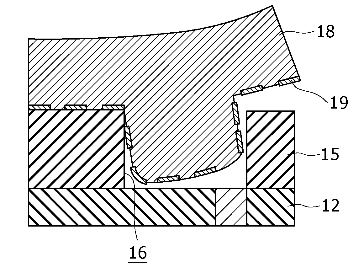
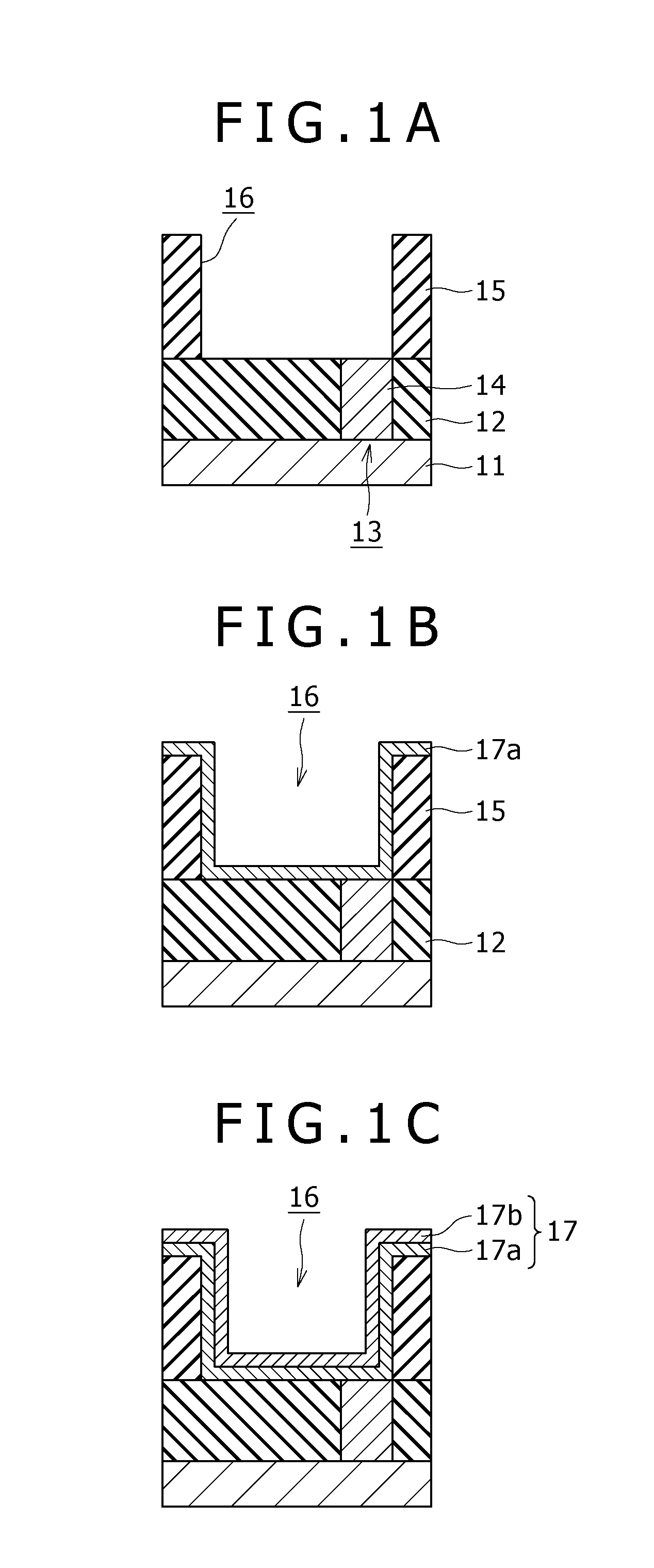
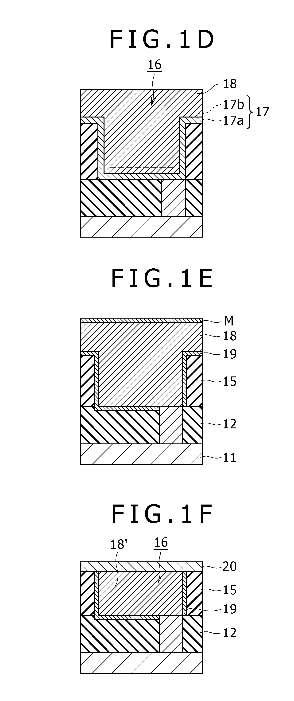
[0023]A method for manufacturing a semiconductor device according to a first embodiment of the present invention relates to formation of a single damascene interconnect structure. The first embodiment will be described below with reference to FIGS. 1A to 1F as sectional views of manufacturing steps. In the following description, the same components as those in the related art are given the same numerals.

[0024]Referring initially to FIG. 1A, an interlayer insulating film 12 composed of e.g. SiO2 is formed on a substrate 11 formed of a silicon wafer on which elements such as transistors are formed. Thereafter, a via hole 13 reaching the substrate 11 is formed, and then a via 14 composed of e.g. W is buried in the via hole 13.

[0025]Subsequently, by e.g. plasma enhanced chemical vapor deposition (PECVD) with use of silane (SiH4) as the deposition gas, an interlayer insulating film 15 composed of e.g. SiO2 is formed on the interlayer insulating film 12 and the via 14.

[0026]Subsequently, ...

second embodiment

[0044]A method for manufacturing a semiconductor device according to a second embodiment of the present invention will be described below with reference to FIGS. 2A to 2K as sectional views of manufacturing steps. For the description of the method according to the second embodiment, an example in which a dual damascene interconnect structure is formed over the cap film described in the first embodiment will be described.

[0045]Referring initially to FIG. 2A, on the cap film 20, an interlayer insulating film 21 composed of e.g. SiO2 is deposited to a film thickness of 350 nm by e.g. PE-CVD. Subsequently, a resist pattern (not shown) having a via hole pattern is formed on the interlayer insulating film 21, and then a via hole 22a reaching the cap film 20 is formed by etching with use of this resist pattern as the mask.

[0046]Referring next to FIG. 2B, a resist R is applied on the interlayer insulating film 21 in such a manner as to fill the via hole 22a. Subsequently, a spin-on-glass (S...


PUM

PropertyMeasurementUnit
thicknessaaaaaaaaaa
thicknessaaaaaaaaaa
thicknessaaaaaaaaaa

Abstract

Disclosed herein is a method for manufacturing a semiconductor device, the method including the steps of: forming a recess in an insulating film provided over a substrate; forming a plating seed layer in such a way that an inner wall of the recess is covered, the plating seed layer arising from sequential deposition of an alloy layer composed of copper and a metal other than copper and a conductive layer composed mainly of copper; burying a conductive layer composed mainly of copper by plating in the recess on which the plating seed layer is provided; and carrying out heat treatment to cause the metal in the alloy layer to react with a constituent in the insulating film, to thereby form a barrier film composed of a metal compound having a copper diffusion barrier function at an interface between the alloy layer and the insulating film.

Description

CROSS REFERENCES TO RELATED APPLICATIONS[0001]The present invention contains subject matter related to Japanese Patent Application JP 2006-222194 filed in the Japan Patent Office on Aug. 17, 2006, the entire contents of which being incorporated herein by reference.BACKGROUND OF THE INVENTION[0002]1. Field of the Invention[0003]The present invention relates to a method for manufacturing a semiconductor device, and particularly to a method for manufacturing a semiconductor device that has a damascene structure in which a self-formed barrier film is provided between an interconnect or via and an interlayer insulating film.[0004]2. Description of the Related Art[0005]In a general process for forming a copper (Cu) interconnect in a semiconductor device, a damascene method is employed, in which an interconnect pattern is formed by filling an interconnect trench provided in an interlayer insulating film. In formation of a Cu interconnect by use of the damascene method, generally before bur...

Claims


Application Information

Patent Timeline
Patent Type & Authority Applications(United States)
IPC IPC(8): C25D5/02
CPCH01L21/76808H01L21/76831H01L21/76843H01L21/76844H01L2221/1089H01L21/76867H01L21/76873H01L23/53238H01L23/53295H01L21/76864H01L2924/0002H01L2924/00H01L21/28
Inventor OHBA, YOSHIYUKIHAYASHI, TOSHIHIKO
Owner SONY CORP
Why Eureka
Try Eureka