Hybrid interconnect structure for performance improvement and reliability enhancement

a hybrid interconnect and performance improvement technology, applied in the field of hybrid interconnect structures, can solve the problems of poor conductor fill property, poor performance of low-k dielectric materials, and inability of physical vapor deposition (pvd) diffusion barrier deposition technology to offer reasonable coverage on the surface of porous low-k dielectric materials, etc., to achieve improved reliability and performance, improve process control, and high volume manufacturing

Active Publication Date: 2008-07-24
TAIWAN SEMICON MFG CO LTD
View PDF40 Cites 56 Cited by
  • Summary
  • Abstract
  • Description
  • Claims
  • Application Information

AI Technical Summary

Benefits of technology

[0010]The present invention provides an interconnect structure (of the single or dual damascene type) and a method of forming the same, in which a dense (i.e., non-porous) dielectric spacer is present on the sidewalls of a dielectric material. The presence of the dense dielectric spacer results in a hybrid interconnect structure that has improved reliability and performance as compared with existing prior art interconnect structures which do not include such dense dielectric spacers. Moreover, the inventive hybrid interconnect structure provides for better process control which leads to the potential for high volume manufacturing.

Problems solved by technology

Additionally, it is a significant challenge for current interconnects processing to integrate porous low-k dielectric materials with other module processes.
For example, the conventional chemical mechanical polishing (CMP) process has difficulty in planarizing a low mechanical-module porous dielectric, and the conventional physical vapor deposition (PVD) diffusion barrier deposition technology cannot offer reasonable coverage on the surface of the porous low-k dielectric material.
This undercut profile results in poor conductor fill property in the final interconnect structure and leaves voids between the diffusion barrier and the interconnect conductive material.
Reliability related issues may be caused by having the voids present inside the interconnect structure.

Method used


Image

  • Hybrid interconnect structure for performance improvement and reliability enhancement
  • Hybrid interconnect structure for performance improvement and reliability enhancement
  • Hybrid interconnect structure for performance improvement and reliability enhancement

Examples


Embodiment Construction

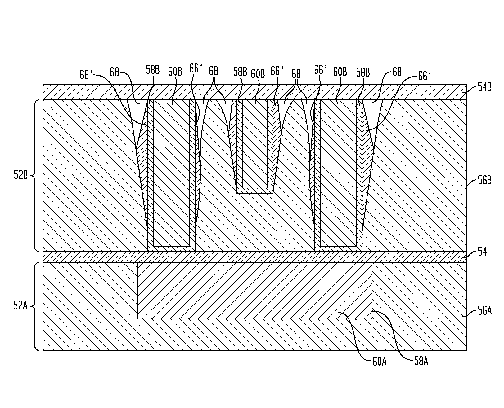
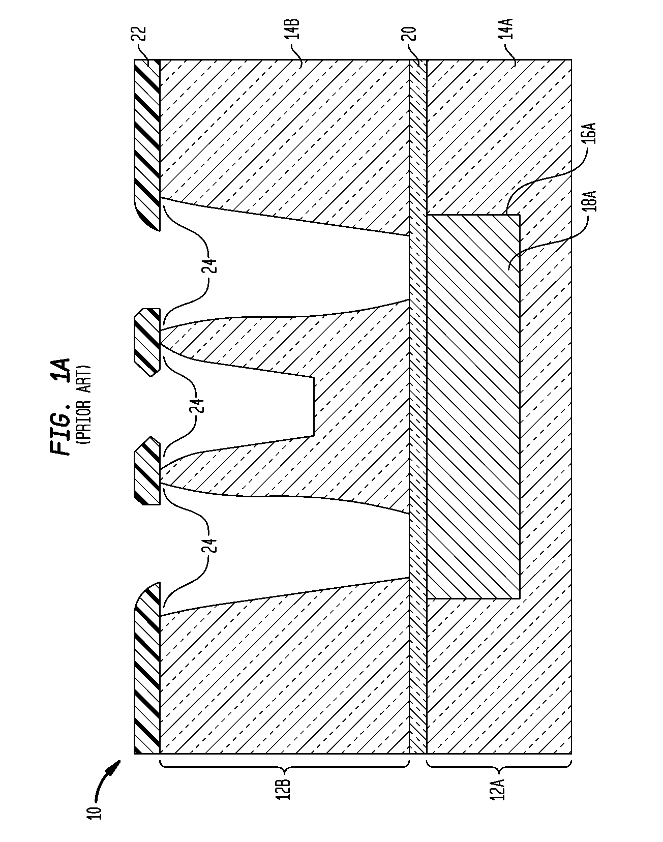
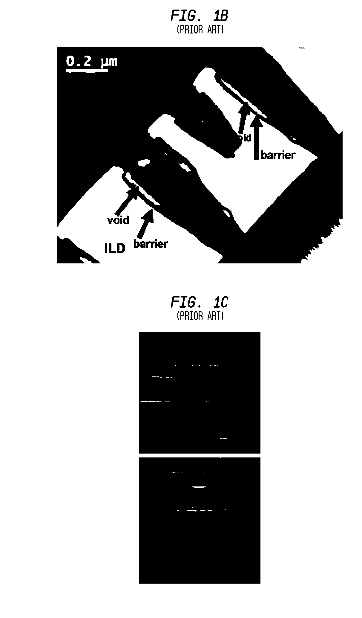
[0027]The present invention, which provides a hybrid interconnect structure including a dense dielectric spacer on sidewalls of a patterned dielectric material as well as a method of fabricating the same, will now be described in greater detail by referring to the following discussion and drawings that accompany the present application. The drawings of the present invention, which are referred to in the present application, are provided for illustrative purposes and, as such, they are not drawn to scale.

[0028]In the following description, numerous specific details are set forth, such as particular structures, components, materials, dimensions, processing steps and techniques, in order to provide a thorough understanding of the present invention. However, it will be appreciated by one of ordinary skill in the art that the invention may be practiced without these specific details. In other instances, well-known structures or processing steps have not been described in detail in order ...


PUM

PropertyMeasurementUnit
dielectric constantaaaaaaaaaa

Abstract

The present invention provides an interconnect structure (of the single or dual damascene type) and a method of forming the same, in which a dense (i.e., non-porous) dielectric spacer is present on the sidewalls of a dielectric material. More specifically, the inventive structure includes a dielectric material having a conductive material embedded within at least one opening in the dielectric material, wherein the conductive material is laterally spaced apart from the dielectric material by a diffusion barrier, a dense dielectric spacer and, optionally, an air gap. The presence of the dense dielectric spacer results in a hybrid interconnect structure that has improved reliability and performance as compared with existing prior art interconnect structures which do not include such dense dielectric spacers. Moreover, the inventive hybrid interconnect structure provides for better process control which leads to the potential for high volume manufacturing.

Description

FIELD OF THE INVENTION [0001]The present invention relates to a semiconductor structure and a method of fabricating the same. More particularly, the present invention relates to a hybrid interconnect structure that exhibits improved performance as well as enhanced reliability.BACKGROUND OF THE INVENTION [0002]Generally, semiconductor devices include a plurality of circuits that form an integrated circuit (IC) fabricated on a semiconductor substrate. A complex network of signal paths will normally be routed to connect the circuit elements distributed on the surface of the substrate. Efficient routing of these signals across the device requires formation of multilevel or multilayered schemes, such as, for example, single or dual damascene wiring structures. The wiring structure typically includes copper, Cu, since Cu based interconnects provide higher speed signal transmission between large numbers of transistors on a complex semiconductor chip as compared with aluminum, Al, based int...

Claims


Application Information

Patent Timeline
Patent Type & Authority Applications(United States)
IPC IPC(8): H01L23/52H01L21/4763
CPCH01L21/7682H01L21/76831H01L23/5222H01L23/53223H01L23/53238H01L23/53266H01L23/53271H01L2924/0002H01L23/5329H01L23/53295H01L21/76841H01L23/481H01L2924/00H01L21/3205H01L21/768H01L23/48
Inventor YANG, CHIH-CHAOSHAW, THOMAS M.WONG, KEITH KWONG HONYANG, HAINING S.
Owner TAIWAN SEMICON MFG CO LTD
Why Eureka
Try Eureka