Semiconductor memory device and method of manufacturing the same

a memory device and semiconductor technology, applied in semiconductor devices, capacitors, electrical equipment, etc., can solve the problems of low electrical resistance of silicon layer over a large area, and achieve the effect of low electrical resistance and high product yield

Inactive Publication Date: 2008-07-31
LONGITUDE SEMICON S A R L
View PDF4 Cites 7 Cited by
  • Summary
  • Abstract
  • Description
  • Claims
  • Application Information

AI Technical Summary

Benefits of technology

[0021]The present invention has been made to overcome the above problems, and it is an object of the present invention to provide a semiconductor memory device and a method of manufacturing the same, which are capa

Problems solved by technology

According to this configuration, even when coating conditions of the lower metal electrode are poor, a silicide layer having low electrical resistance is formed over a large area,

Method used


Image

  • Semiconductor memory device and method of manufacturing the same
  • Semiconductor memory device and method of manufacturing the same
  • Semiconductor memory device and method of manufacturing the same

Examples


Embodiment Construction

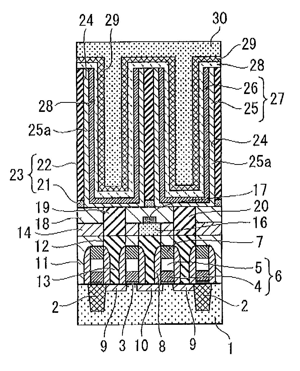
[0047]Hereinafter, a semiconductor memory device and a semiconductor memory device manufacturing method according to an embodiment of the present invention will be described.

[0048]FIG. 1 is a cross-sectional view showing a semiconductor memory device according to an embodiment of the present invention. In this figure, a semiconductor substrate 1 is formed of a semiconductor, for example, silicon, containing impurities of a predetermined concentration.

[0049]Device isolation regions 2 isolating a transistor (selection transistor) are formed in regions other than transistor formation regions on the semiconductor substrate 1 by a STI (Shallow Trench Isolation) method.

[0050]In the transistor formation region, a gate insulating film 3 is formed as a silicon oxide film on the semiconductor substrate 1 by, for example, a thermal oxidation method or the like.

[0051]A gate oxide film 6 is formed by a multilayer laminate of a polycrystalline silicon film 4 and a metal film 5. For the polycrysta...


PUM


Abstract

The semiconductor memory device includes: an interlayer insulating film that is formed on a semiconductor substrate; an insulating film that is formed on the interlayer insulating film and has a cylinder hole; and a capacitor that has an impurity-containing silicon film, a lower metal electrode, a capacitive insulating film and an upper electrode, which are formed so as to cover a bottom and a side of the cylinder hole, wherein the cylinder hole extends through the insulating film so as to expose an end side of the contact plug, the end side facing opposite from the source electrode; and the impurity-containing silicon film has a silicide layer near an interface between the impurity-containing silicon film and the lower metal electrode, the silicide layer being produced by a reaction of impurity-containing silicon included in the impurity-containing silicon film with metal included in the lower metal electrode.

Description

BACKGROUND OF THE INVENTION[0001]Priority is claimed on Japanese Patent Application No. 2007-22399, filed Jan. 31, 2007, the contents of which are incorporated herein by reference.FIELD OF THE INVENTION[0002]This invention relates to a semiconductor memory device having a capacitor stacked, in the form of a cylinder, on a semiconductor substrate, which is called a stacked capacitor, for use in, for example, a dynamic random access memory (DRAM), and a method of manufacturing the same.DESCRIPTION OF THE RELATED ART[0003]As a memory cell used in a DRAM (Dynamic Random Access Memory) has become smaller with miniaturization of a semiconductor device, it has become difficult to secure sufficient capacitance. However, a certain level of capacitance is required to secure stable operation and reliability of the DRAM. Accordingly, in order to secure a surface area, which is one of the factors to define capacitance, efforts have been made to increase capacitance by using a three-dimensional s...

Claims


Application Information

Patent Timeline
IPC IPC(8): H01L27/108H01L21/02
CPCH01L27/10814H01L28/91H01L27/10852H10B12/315H10B12/033
Inventor SUGIOKA, SHIGERU
Owner LONGITUDE SEMICON S A R L
Why Eureka
Try Eureka