Manufacturing method of semiconductor device using sti technique

a manufacturing method and semiconductor technology, applied in semiconductor/solid-state device manufacturing, basic electric elements, electric devices, etc., can solve the problems of increasing the difficulty in increasing the difficulty of downsizing the device, and increasing the difficulty of forming the isolation region

Inactive Publication Date: 2008-07-31
KK TOSHIBA
View PDF6 Cites 246 Cited by
  • Summary
  • Abstract
  • Description
  • Claims
  • Application Information

AI Technical Summary

Benefits of technology

[0013]According to a first aspect of the present invention, there is provided a manufacturing method of a semiconductor device comprising simultaneously forming a first isolation trench and a second isolation trench having width larger than the first isolation trench in a main surface area of a semiconductor substrate, narrowing width of an opening portion of the first isolation trench by forming a first insulating film on the main surface of the semiconductor substrate and in the first and second isolation trenches, forming void in the first isolation trench while covering the opening portion of the first isolation trench by forming a second insulating film on the first insulating film by use of a high-density plasma-CVD method and filling the second isolation trench with the second insulating film, removing part of the second insulating film which covers the opening portion by anisotropic etching, and filling the void with an insulating film having fluidity at the film formation period.

Problems solved by technology

Thus, it is predicted that downsizing of the devices is further developed in the future although the technical difficulty is increased.
The width of the trench formed by the STI technique reaches the trench width of 0.1 μm or less, for example, approximately 90 to 65 nm, but the degree of difficulty in forming the isolation region is rapidly increased in accordance with downsizing.
That is, since the width of the STI trench is reduced due to miniaturization although it is desired to keep the depth of the STI trench at least substantially constant, the aspect ratio of the trench which is filled with the insulating film becomes higher for every downsized generation and the trench filling technique rapidly becomes more difficult.
Particularly, when the half pitch is reduced from 45 to 32 nm in the future, it will become extremely difficult to fill with a silicon oxide film formed by a conventional high-density plasma (HDP)-CVD method, since almost no HDP-CVD deposition occurs in the STI trench when the width of the STI trench becomes less than 30 nm although HDP-CVD method is originally a highly anisotropic film formation method.
However, the film density of the flowable insulating film is generally low, a lot of impurities such as C, N, H are contained in the film and the processing resistance thereof is low.
Particularly, there is a problem that the wet etching rate is high.
In order to solve the above problem, a method for improving the film quality by the heat treatment in the steam atmosphere is generally used, but in the generation of the half pitch of 45 to 32 nm, there occurs a problem that the element region itself is oxidized by oxidation in the steam atmosphere and the width thereof is reduced and it is difficult to sufficiently improve the film quality.
Further, since the flowable film shrinkage is generally large, high tensile stress tends to occur and there occurs a problem that deformation and crystalline defects occur due to stress of the STI region in the narrow active area.
Further, since the stress has correlation with the volume of the formed insulating film, there occurs a problem that cracking of the film will occur due to the strong stress in the large STI region.

Method used


Image

  • Manufacturing method of semiconductor device using sti technique
  • Manufacturing method of semiconductor device using sti technique
  • Manufacturing method of semiconductor device using sti technique

Examples


first embodiment

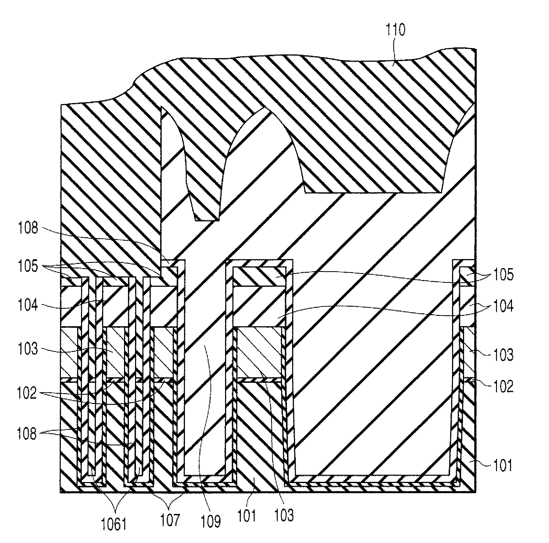
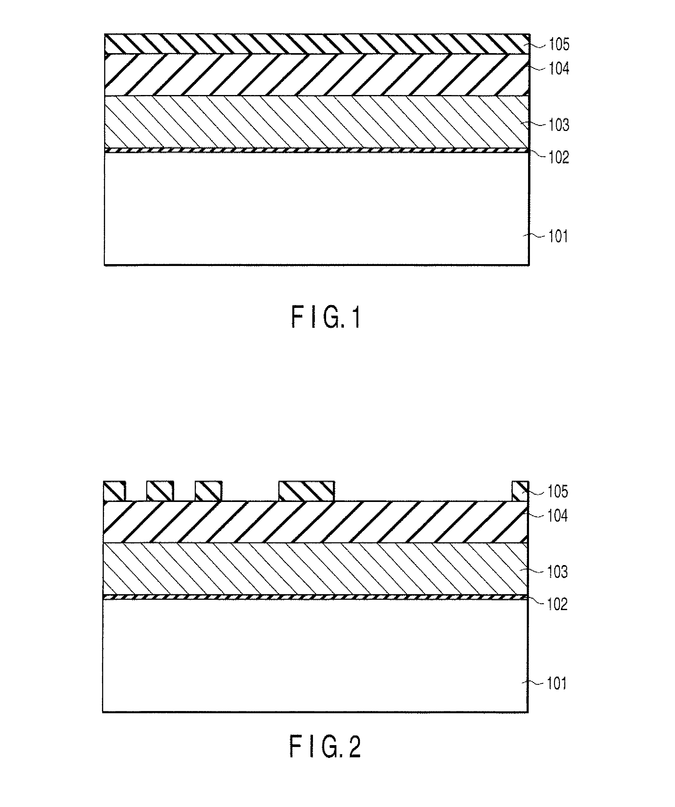
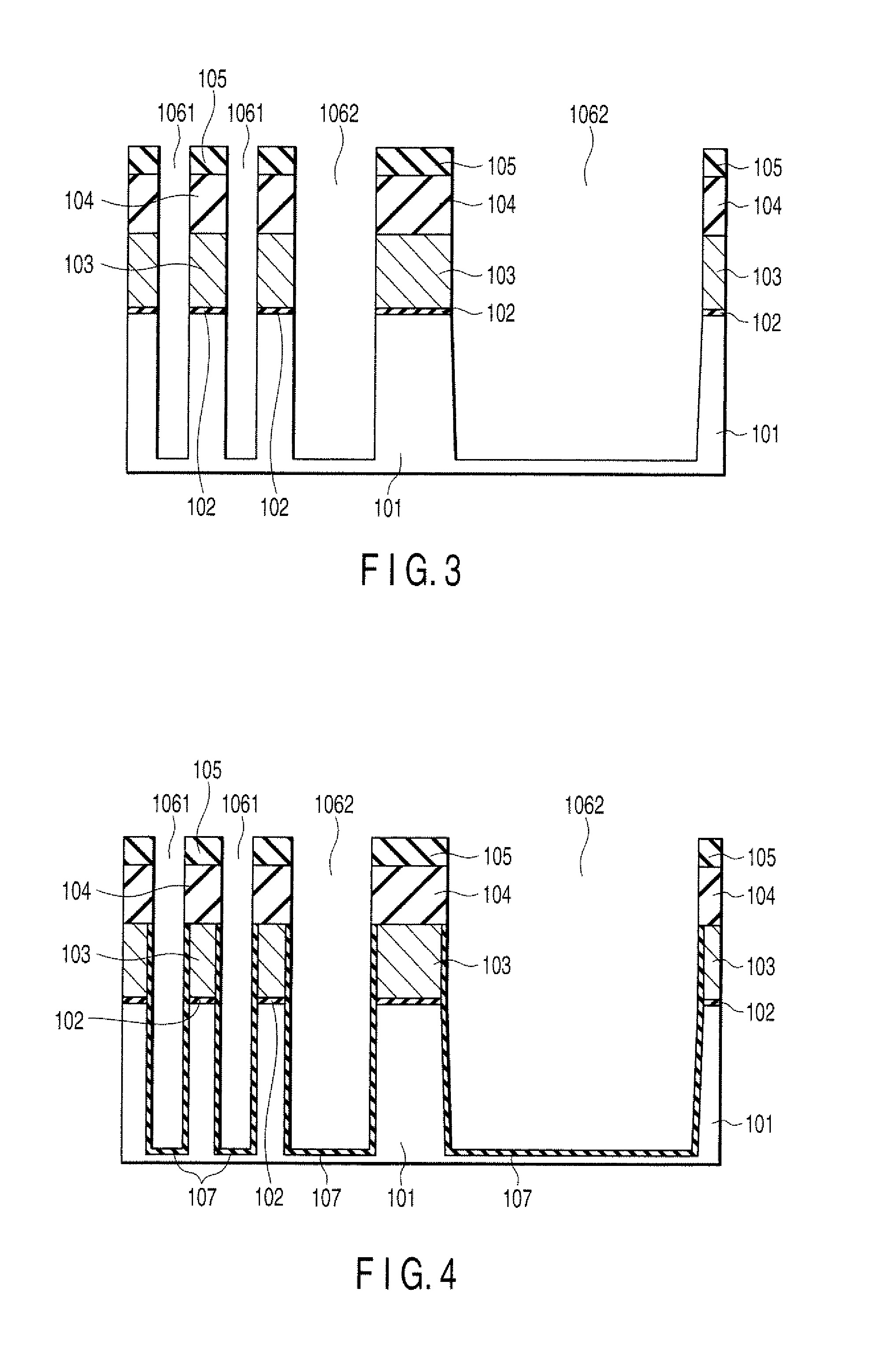
[0103]A manufacturing method of a semiconductor device according to a first embodiment of this invention is explained with reference to FIGS. 1 to 14.

[0104]The present embodiment is one example of a manufacturing method of a flash memory and indicates a case wherein a gate insulating film and a gate electrode film used as floating gates are previously formed on a semiconductor substrate and then STI regions are formed.

[0105]First, as shown in FIG. 1, a silicon thermal oxynitride film 102 used as a gate insulating film is formed to a thickness of approximately 8 nm on a semiconductor substrate 101, a P-doped polysilicon film 103 used as floating gates is formed to a thickness of approximately 120 nm and a silicon nitride film 104 used as a polishing stopper for a chemical mechanical polishing (CMP) process is formed to a thickness of approximately 100 nm. Then, a CVD silicon oxide film 105 used as a mask for reactive ion etching (RIE) is formed on the entire surface of the silicon ni...

second embodiment

[0138]A manufacturing method of a semiconductor device according to a second embodiment of this invention is explained with reference to FIGS. 15 to 30.

[0139]The present embodiment is one example of a manufacturing method of a logic device and, in this case, STI regions are first formed on a semiconductor substrate and then transistors are formed. In the present embodiment, the manufacturing method for realizing an STI structure which is resistant to wet etching in the multi-gate oxide process is shown.

[0140]First, as shown in FIG. 15, a silicon oxide film 202 used as a buffer film is formed to 2 nm on a semiconductor substrate 201 and a silicon nitride film 203 used as a CMP polishing stopper is formed to 100 nm. Then, a CVD silicon oxide film 230 used as a mask for reactive ion etching (RIE) is formed on the entire surface of the silicon nitride film 203 (FIG. 15) and a photoresist film is further coated (not shown).

[0141]Next, the photoresist film is processed by use of the norma...

third embodiment

[0164]A manufacturing method of a semiconductor device according to a third embodiment of this invention is explained with reference to FIGS. 31 to 50.

[0165]The present embodiment is one example of a manufacturing method of a flash memory and, in this case, a gate insulating film and gate electrode film used as floating gates are previously formed on a semiconductor substrate and then STI of the cell portion are formed. After this, a silicon nitride film used as a barrier film which protects the cell portion is formed and then STI regions in a peripheral portion are formed.

[0166]First, as shown in FIG. 31, a silicon thermal oxynitride film 302 used as a gate insulating film is formed to a thickness of approximately 8 nm on a semiconductor substrate 301, a P-doped polysilicon film 303 used as floating gates is formed to a thickness of approximately 120 nm and a silicon nitride film 304 used as a polishing stopper for the CMP process is formed to a thickness of approximately 60 nm. Th...


PUM


Abstract

A first trench and a second trench having width wider than the first trench are simultaneously formed in a main surface area of a semiconductor substrate. The width of an opening portion of the first trench is made narrower by forming a first insulating film on the main surface of the semiconductor substrate and in the first and second trenches. A second insulating film is formed on the first insulating film by use of a high-density plasma-CVD method to form a void in the first trench while covering the opening portion of the first trench, and the second trench is filled with the second insulating film. Then, part of the second insulating film which covers the opening portion is removed by anisotropic etching and the void is filled with an insulating film having fluidity at the film formation time.

Description

CROSS-REFERENCE TO RELATED APPLICATIONS[0001]This application is based upon and claims the benefit of priority from prior Japanese Patent Application No. 2006286917, filed Oct. 20, 2006, the entire contents of which are incorporated herein by reference.BACKGROUND OF THE INVENTION[0002]1. Field of the Invention[0003]This invention relates to a manufacturing method of a semiconductor device using the shallow trench isolation (STI) technique for formation of an element isolation region.[0004]2. Description of the Related Art[0005]The technique for fine patterning of LSIs is rapidly developed to enhance the performance of devices due to high integration density (enhance the operation speed and lower the power consumption) and suppress the manufacturing cost. In recent years, memory elements in which the minimum processing dimension is 90 nm are produced in the case of mass production. Further, in the case of a logic device at the development stage, devices whose gale length is reduced t...

Claims


Application Information

Patent Timeline
Patent Type & Authority Applications(United States)
IPC IPC(8): H01L21/76
CPCH01L21/76229
Inventor KIYOTOSHI, MASAHIRO
Owner KK TOSHIBA
Why Eureka
Try Eureka