Display driver IC having embedded dram
a display driver and embedded dram technology, applied in the field of display driver ic, can solve the problems of ic chip having the strip shape susceptible to stress, end product may become malfunctioning depending, and the display driver ic may not work properly, so as to improve the yield, and improve the data retention characteristic
- Summary
- Abstract
- Description
- Claims
- Application Information
AI Technical Summary
Benefits of technology
Problems solved by technology
Method used
Image
Examples
first embodiment
1. First Embodiment
1-1. Overall Configuration
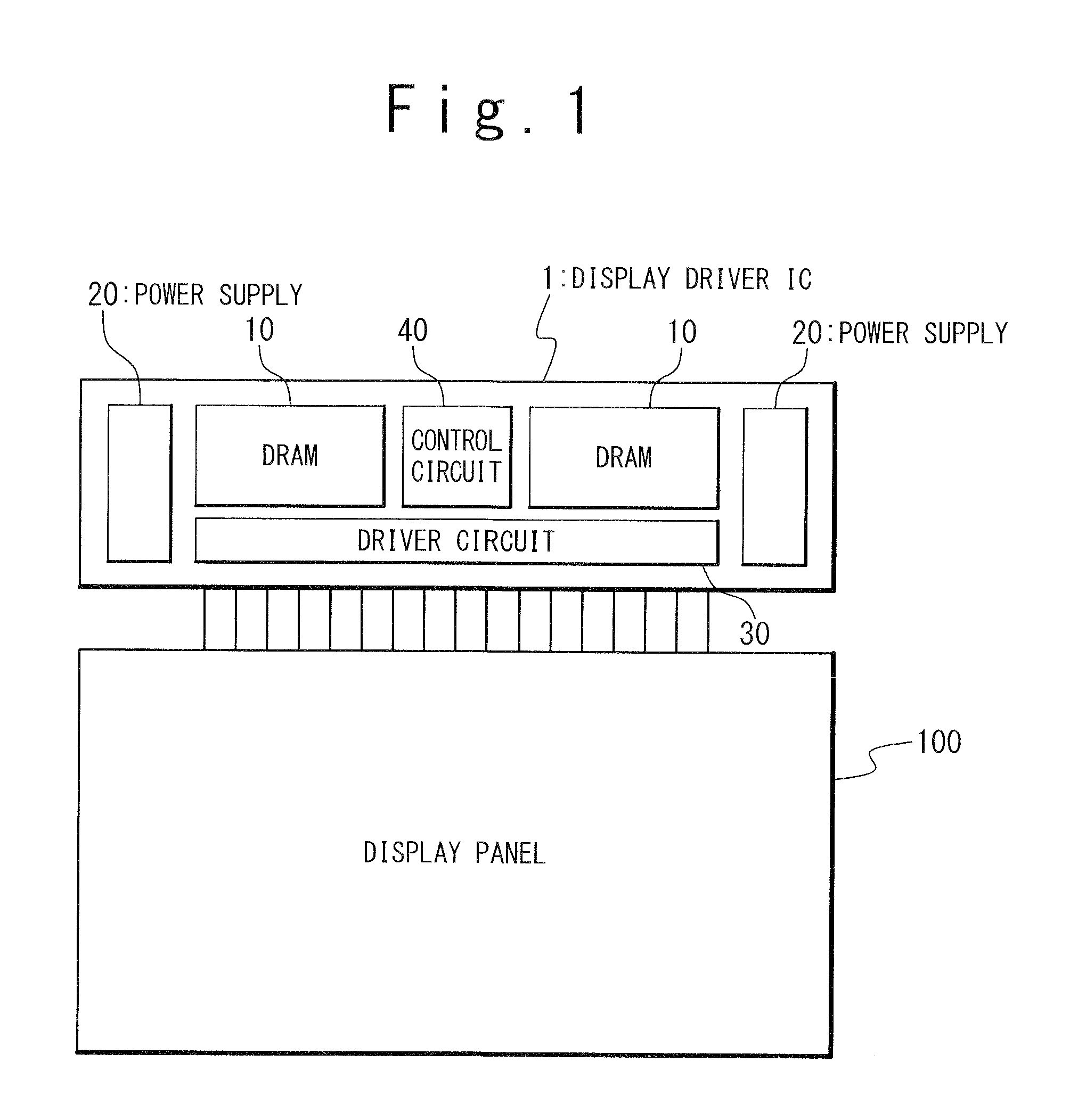
[0030]FIG. 1 illustrates a layout of a display driver IC 1 according to the embodiments of the present invention. The display driver IC 1 is an integrated circuit for controlling display of an image on a display panel 100. The display driver IC 1 is provided with an embedded DRAM 10, a power supply circuit 20, a driver circuit 30, a display control circuit 40 and the like. The display driver IC 1 is integrated on a single chip. As shown in FIG. 1, the display driver IC chip is long from side to side, i.e., the display driver IC chip has a “strip shape”. Such a strip shape is peculiar to the display driver IC used in the image display apparatus.
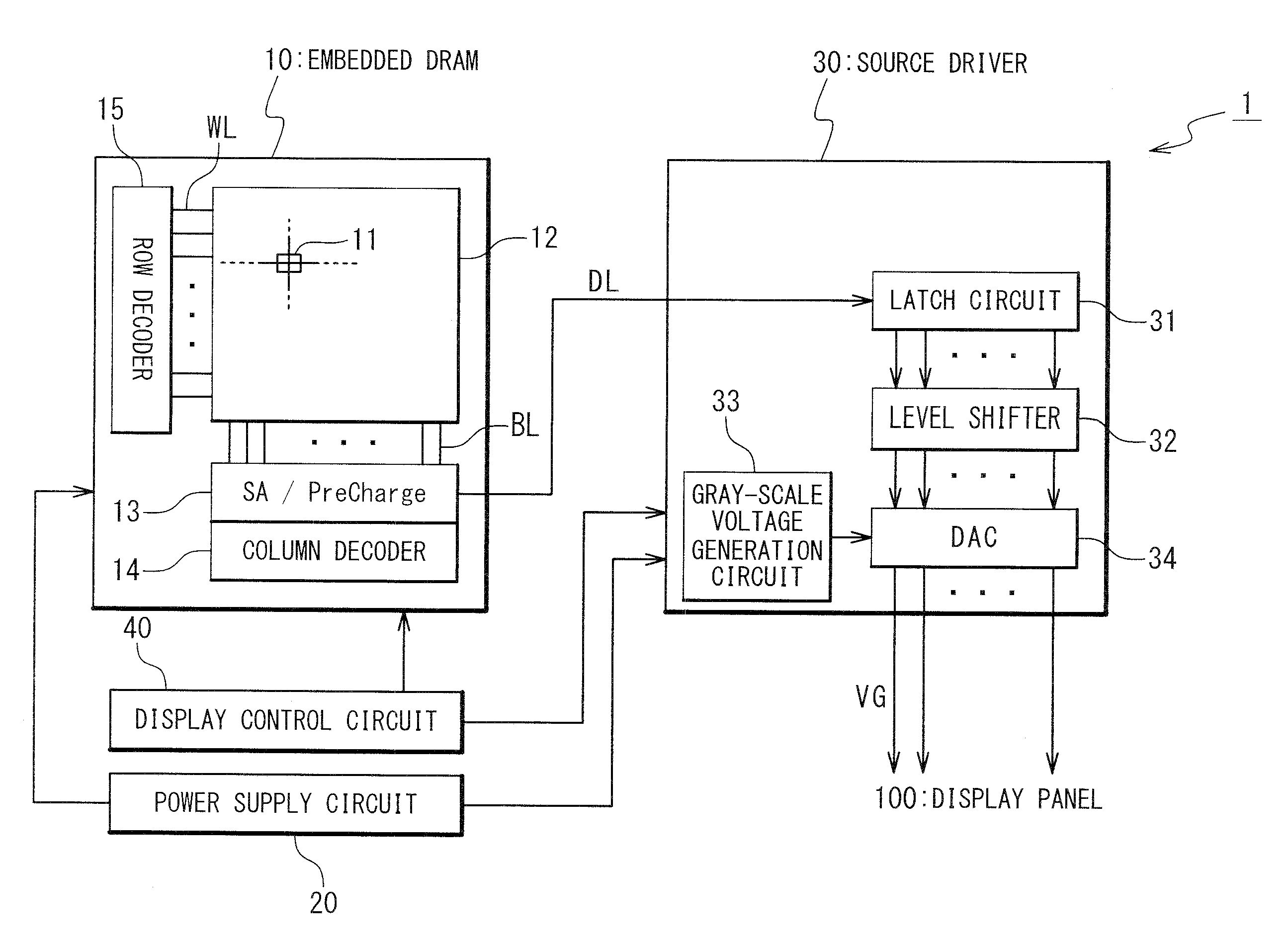
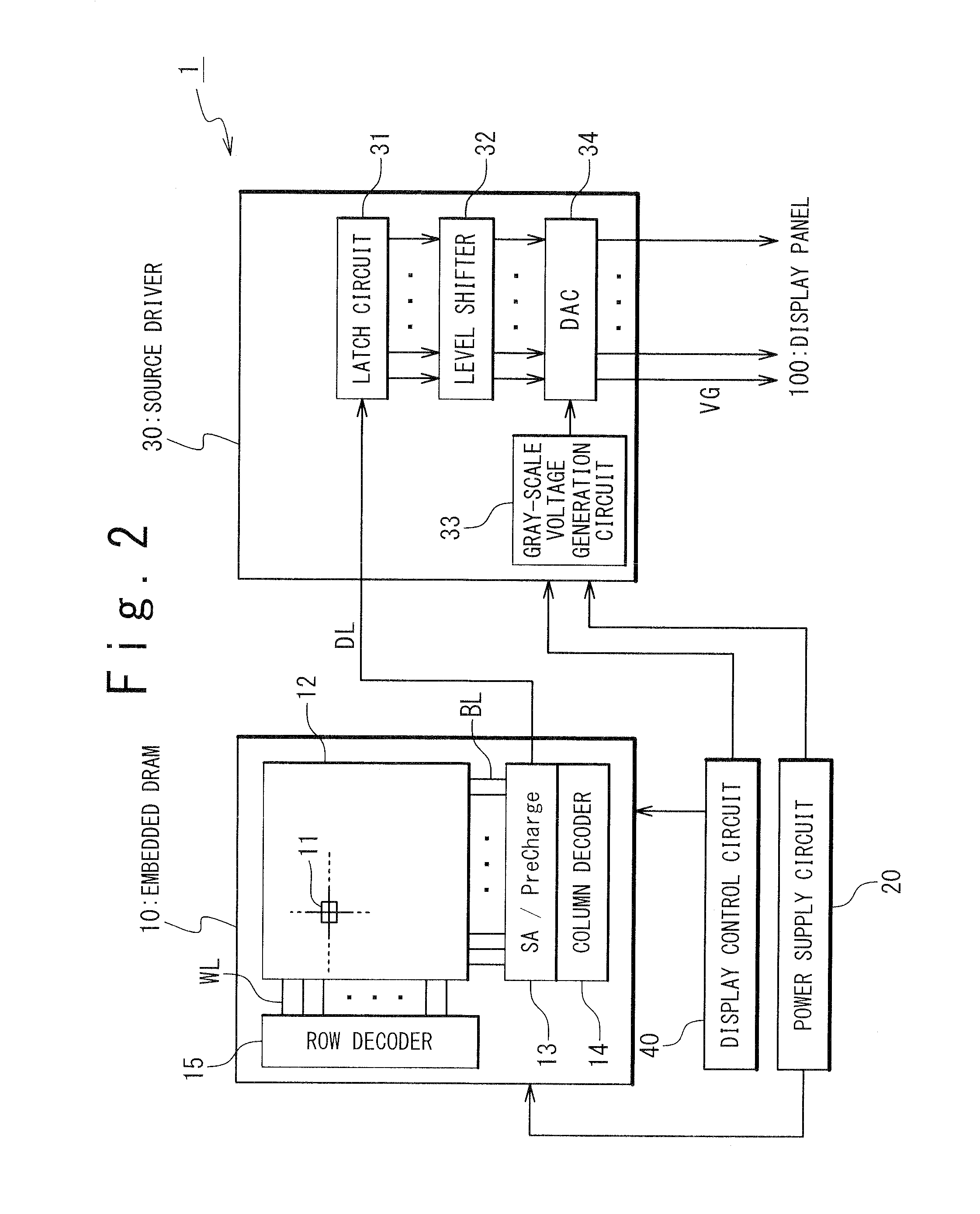
[0031]FIG. 2 is a block diagram showing a circuit configuration of the display driver IC 1 according to the present embodiment. In FIG. 2, a source driver 30 connected to source lines of the display panel 100 is illustrated as the above-mentioned driver circuit 30.
[0032]The embedded DRAM 10 is used ...
second embodiment
2. Second Embodiment
[0049]As described above, the chip area of the display driver IC can be reduced by replacing an embedded SRAM with an embedded DRAM. However, in the case where the access unit of the data reading / writing is the twin cell, a memory cell array area required for the same storage capacity doubles as compared with a case where the access unit is a single cell, which weakens the chip area reduction effect. It is therefore preferable to make an area of one DRAM cell as small as possible. The layout structure of the memory cells 11 shown in the foregoing FIG. 3 is the so-called “8F2 cell” structure. In a second embodiment of the present invention, a “6F2 cell” structure is employed instead of the “8F2 cell” structure.
[0050]FIG. 6 is a circuit diagram showing a part of a memory cell array 12 of an embedded DRAM 10′ according to the second embodiment. Memory cells 11-00A to 11-01B are connected to a word line WL0, while memory cells 11-10A to 11-11B are connected to a word...
PUM
 Abstract
Description
Claims
Application Information


