Metal-insulator-metal capacitor and fabrication method thereof
- Summary
- Abstract
- Description
- Claims
- Application Information
AI Technical Summary
Benefits of technology
Problems solved by technology
Method used
Image
Examples
first embodiment
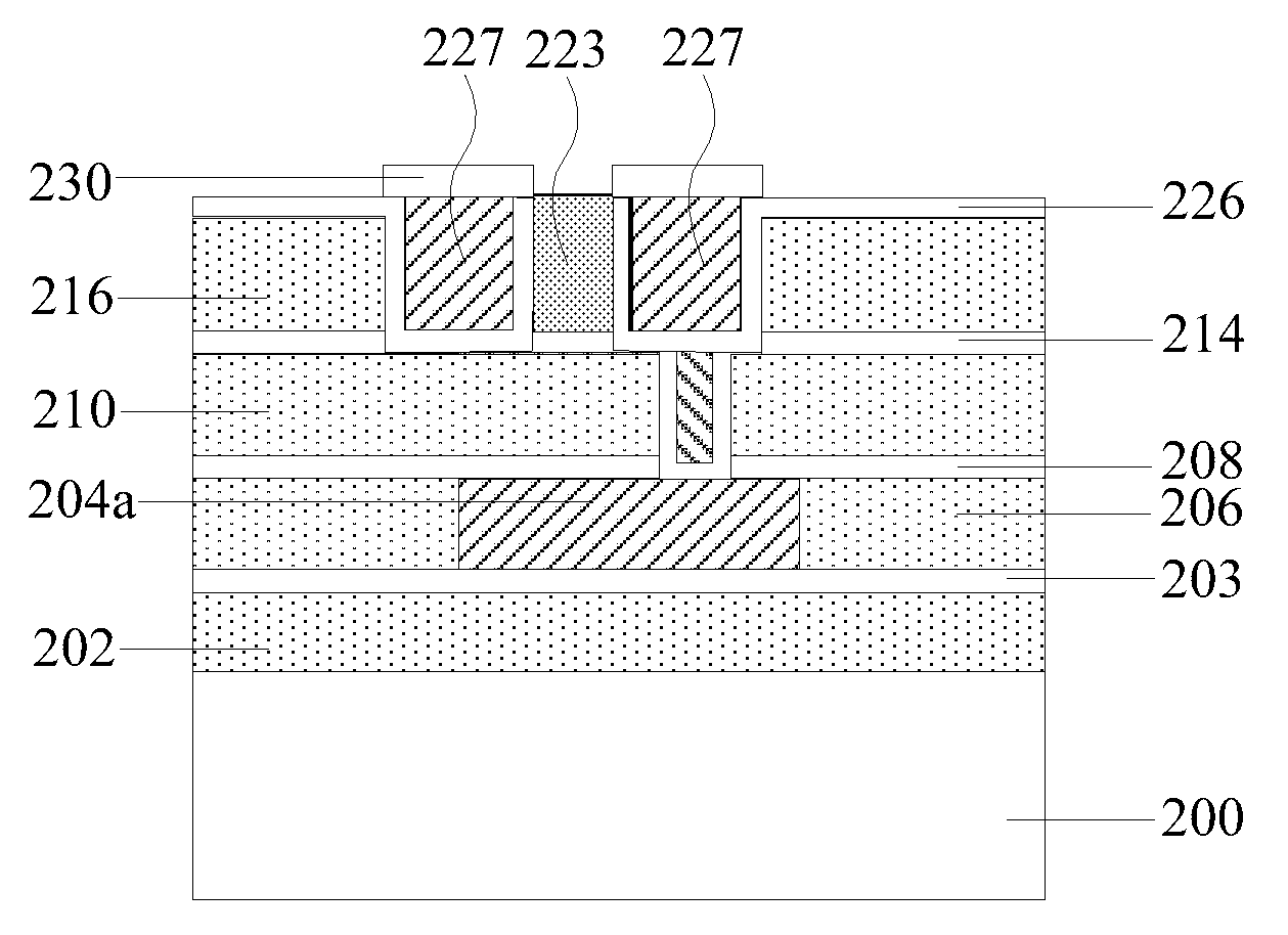
[0029]FIG. 7 is a flow diagram illustrating a method for fabricating metal-insulator-metal capacitor according to the present invention. As shown in FIG. 7, an interlayer dielectric layer is formed on a semiconductor substrate by carrying out the step S201.
[0030]In this embodiment, the interlayer dielectric layer is made of silicon oxide or Borophosphosilicate Glass (BPSG) and the manner of forming the interlayer dielectric layer is the well-known chemical vapor deposition.
[0031]An insulation trench is formed in the interlayer dielectric layer to run through the interlayer dielectric layer and allow semiconductor substrate to be exposed by carrying out the step S202.
[0032]In this embodiment, the insulation trench is formed by dry etching the interlayer dielectric layer until the semiconductor substrate is exposed.
[0033]The insulation trench is filled with insulation material to form an insulation structure by carrying out the step S203.
[0034]In this embodiment, the insulation materi...
second embodiment
[0039]FIG. 8 is a flow diagram illustrating a method for fabricating metal-insulator-metal capacitor according to the present invention. As shown in FIG. 8, an interlayer dielectric layer is formed on a semiconductor substrate by carrying out the step S301.
[0040]In this embodiment, the interlayer dielectric layer is made of silicon oxide or Borophosphosilicate Glass (BPSG) and the manner of forming the interlayer dielectric layer is the well-known chemical vapor deposition.
[0041]Two metal trenches are formed in the interlayer dielectric layer to run through the interlayer dielectric layer and allow the semiconductor substrate to be exposed by carrying out the step S302.
[0042]In this embodiment, the metal trenches are formed by dry etching the interlayer dielectric layer until the semiconductor substrate is exposed.
[0043]The metal trenches are filled with metal material to form the electrodes of the capacitor by carrying out the step S303.
[0044]In this embodiment, the metal material ...
PUM
 Abstract
Description
Claims
Application Information
 - Generate Ideas
- Intellectual Property
- Life Sciences
- Materials
- Tech Scout
- Unparalleled Data Quality
- Higher Quality Content
- 60% Fewer Hallucinations
Browse by: Latest US Patents, China's latest patents, Technical Efficacy Thesaurus, Application Domain, Technology Topic, Popular Technical Reports.
© 2025 PatSnap. All rights reserved.Legal|Privacy policy|Modern Slavery Act Transparency Statement|Sitemap|About US| Contact US: help@patsnap.com


