Method for Forming Solder Bump and Method for Mounting Semiconductor Device

a semiconductor device and solder bump technology, applied in the direction of semiconductor/solid-state device details, sustainable manufacturing/processing, final product manufacturing, etc., can solve the problems of insufficient reduction of the conventional method of reducing the pitch between and increasing the number of connection terminals is difficult to employ, so as to achieve high reliability, easy formation, and high density semiconductor mounting

Active Publication Date: 2008-08-21
PANASONIC CORP
View PDF20 Cites 35 Cited by
  • Summary
  • Abstract
  • Description
  • Claims
  • Application Information

AI Technical Summary

Benefits of technology

[0032]According to the present invention, solder bumps each having a projection or a pit can be easily formed by melting a solder powder included in a resin composition and allowing the melted solder powder to self-assemble on terminals of a plate. Also, since the height of the solder bumps to be formed can be controlled by using the flat plate, the solder bumps in a uniform height can be formed. Therefore, when the solder bumps of this invention are formed on terminals of a semiconductor device and / or a wiring board, it is possible to perform high density semiconductor mounting with high reliability.
[0033]Furthermore, a semiconductor device can be easily and definitely mounted on a wiring board by mutually fitting and connecting solder bumps having projections and / or pits formed according to the invention. Therefore, it is possible to perform semiconductor mounting with high reliability.

Problems solved by technology

Therefore, it is difficult to employ the conventional method for reducing the pitch between and increasing the number of connection terminals.
This method, however, is not sufficient for reducing the pitch between and increasing the number of connection terminals in the same manner as the conventional solder bump connection.

Method used


Image

  • Method for Forming Solder Bump and Method for Mounting Semiconductor Device
  • Method for Forming Solder Bump and Method for Mounting Semiconductor Device
  • Method for Forming Solder Bump and Method for Mounting Semiconductor Device

Examples


embodiment 1

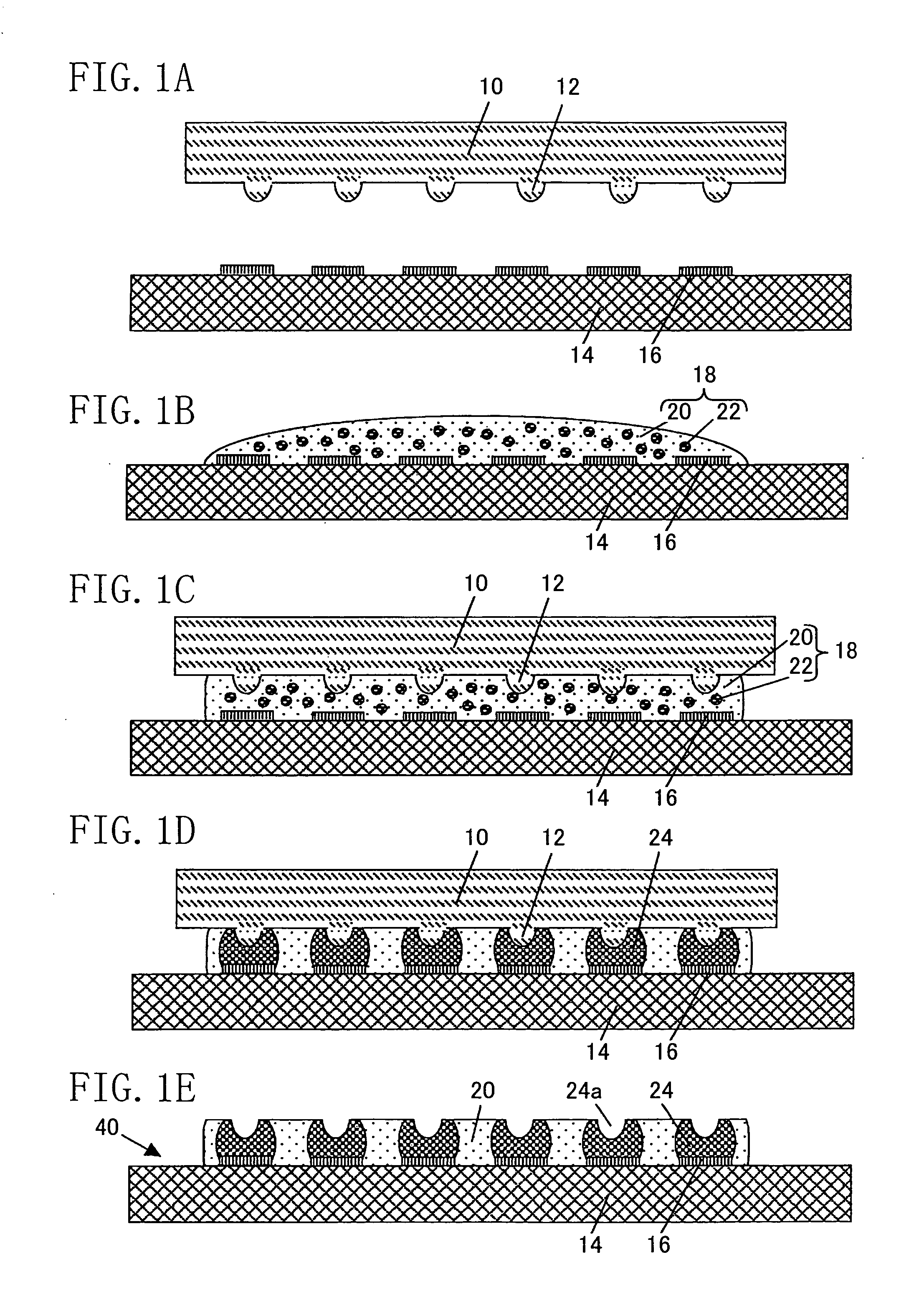
[0063]FIG. 1 shows cross-sectional views for schematically showing procedures in a method for forming solder bumps according to Embodiment 1 of the invention. In this embodiment, a case where a wiring board is used as an electronic component will be described.

[0064]As shown in FIG. 1A, projections 12 are formed on one face of a flat plate 10 in positions corresponding to terminals 16 for forming bumps of a wiring board 14. Such projections 12 with a constant height can be formed at a given pitch by, for example, forming a given pattern on the flat plate 10 by photolithography process and removing an unwanted portion of the flat plate with this pattern used as a mask by etching, sandblasting or the like. Alternatively, the projections 12 can be formed by a printing method. As the flat plate 10, for example, a glass plate, a ceramic plate, a silicon plate or a plastic plate with heat resistance can be used.

[0065]Furthermore, the wiring board 14 may be a multi-layered board or a double...

embodiment 2

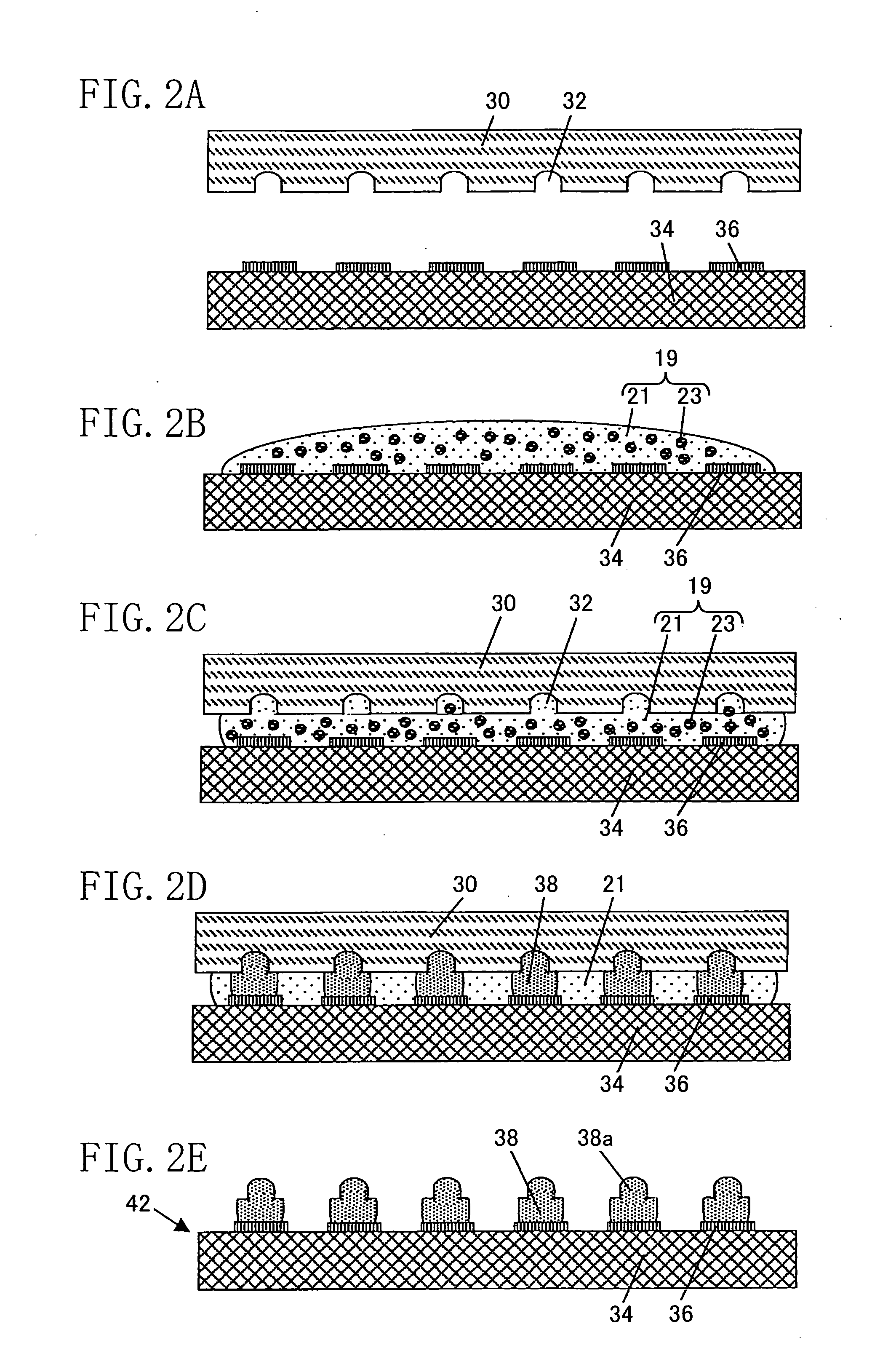
[0082]FIG. 2 shows cross-sectional views for schematically showing procedures in a method for forming solder bumps according to Embodiment 2 of the invention. In this embodiment, a case where a semiconductor device 34 is used as an electronic component will be described. In procedures commonly performed in Embodiment 1, this embodiment is not limited to the description below but any of various conditions, materials and the like described in Embodiment 1 can be appropriately employed.

[0083]As shown in FIG. 2A, recesses 32 are formed on one face of a flat plate 30 in positions corresponding to terminals 36 for forming bumps of the semiconductor device 34. Such recesses 32 with a given depth can be formed at a given pitch by, for example, forming a given pattern on the flat plate 30 by the photolithography process and performing the etching, the sandblasting or the like with this pattern used as a mask. As the flat plate 30, for example, a glass plate, a ceramic plate, a silicon plate ...

embodiment 3

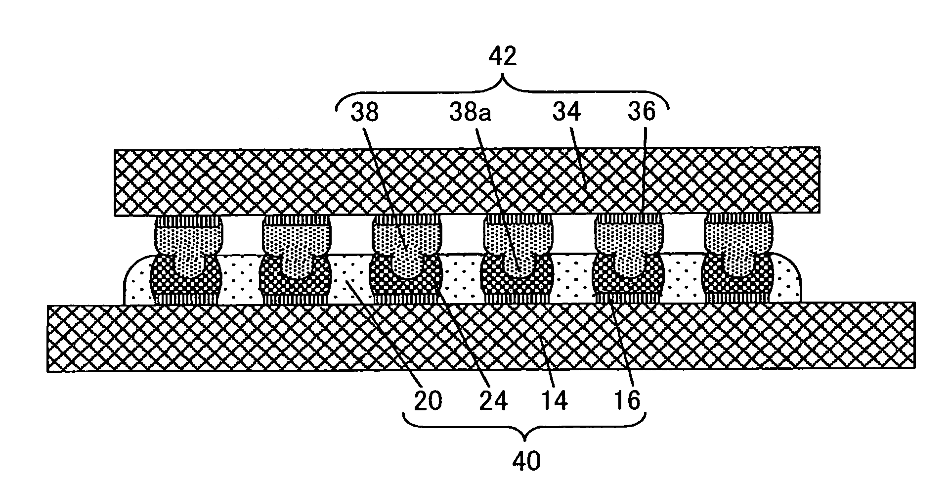
[0103]FIG. 3 shows cross-sectional views for schematically showing procedures in a method for mounting a semiconductor device according to Embodiment 3 of the invention. In the method for mounting a semiconductor device of this embodiment, a solder bump-formed wiring board 40 formed by the method of Embodiment 1 and a solder bump-formed semiconductor device 42 formed by the method of Embodiment 2 are used for the mounting.

[0104]FIG. 3A shows a state where a semiconductor device 34 on which solder bumps 38 each having a projection 38a at the center are formed and a wiring board 14 on which solder bumps 24 each having a pit 24a at the center are formed are aligned. At this point, the inner diameter of the pit 24a is slightly smaller than the outer diameter of the projection 38a. Furthermore, the solder bumps 38 of the semiconductor device 34 are made of a material having a higher melting point than a material used for the solder bumps 24 of the wiring board 12.

[0105]FIG. 3B shows a st...


PUM

PropertyMeasurementUnit
lengthaaaaaaaaaa
temperatureaaaaaaaaaa

Abstract

[Problem] To provide a method for forming solder bumps for realizing high density mounting and a highly reliable method for mounting a semiconductor device.[Means for Solving Problem] A flat plate 10 or 30 having a plurality of projections 12 or recesses 32 thereon is prepared; the flat plate is aligned to oppose an electronic component 14 or 34 and a resin composition 18 or 19 including a solder powder 22 or 23 is supplied to a gap between the flat plate and the electronic component; the resin composition is annealed to melt the solder powder included in the resin composition for growing the solder powder up to the level of the surface of the flat plate by allowing the melted solder powder to self-assemble on terminals 16 or 36, so as to form solder bumps 24 or 38 on the terminals; and the flat plate is removed after cooling and solidifying the solder bumps. Thus, the solder bumps 24 or 38 having pits 24a corresponding to the projections 12 or having projections 38a corresponding to the recesses 32 are formed.

Description

TECHNICAL FIELD[0001]The present invention relates to a method for forming solder bumps for use in mounting a semiconductor device on a wiring board and a method for mounting a semiconductor device having solder bumps formed by the solder bump formation method on a wiring board.BACKGROUND ART[0002]Recently, in accordance with downsizing and improved performance of electronic equipment, signal processing has been developed for digitalization and higher frequencies. Also with respect to semiconductor devices working as core components in such electronic equipment, it is desired to increase the number of connection terminals and reduce the pitch between the connection terminals in accordance with increase of the circuit scale. Furthermore, it has become significant to reduce wiring delay between a semiconductor device and a wiring board and to prevent noise. Therefore, as a connection method between a semiconductor device and a wiring board, a flip-chip mounting method is employed inst...

Claims


Application Information

Patent Timeline
Patent Type & Authority Applications(United States)
IPC IPC(8): B23K31/02B23K1/20
CPCH01L21/4853H01L21/563H01L21/6835H01L23/49816H01L24/11H01L24/12H01L24/16H01L24/81H01L2224/11003H01L2224/13099H01L2224/81193H01L2224/81801H01L2224/83192H01L2924/01009H01L2924/01029H01L2924/0103H01L2924/01033H01L2924/01046H01L2924/01047H01L2924/01049H01L2924/01077H01L2924/01078H01L2924/01079H01L2924/01082H01L2924/09701H05K3/323H05K3/3436H05K3/3484H05K2201/09745H05K2201/10977H05K2203/0108H05K2203/0113H05K2203/043H05K2203/0465H05K2203/167H01L2224/0558H01L2224/05639H01L2224/05644H01L2224/16225H01L2924/01005H01L2924/01006H01L2924/01023H01L2924/01045H01L2924/0105H01L2924/014H01L2224/81141H01L2924/00013H01L2224/32225H01L2224/73204H01L2224/131H01L2224/0401H01L2924/07811H01L2924/00H01L2224/29099H01L2924/15787H01L2924/15788H01L2224/73104H01L2224/1152H05K3/3485Y02P70/50
Inventor KITAE, TAKASHINAKATANI, SEIICHIKOJIMA, TOSHIYUKIKOMATSU, SHINGOYAMASHITA, YOSHIHISA
Owner PANASONIC CORP
Why Eureka
Try Eureka