Organic light-emitting device and display apparatus using the same

a light-emitting device and display device technology, applied in the direction of discharge tube/lamp details, organic semiconductor devices, discharge tubes, etc., can solve the problems of oxidation of electrodes, deterioration of organic compounds, peeling of electrodes/organic substances, etc., to reduce the resonance effect of microcavity structures, and reduce the effect of film thickness variation

Active Publication Date: 2008-08-28
CANON KK
View PDF9 Cites 69 Cited by
  • Summary
  • Abstract
  • Description
  • Claims
  • Application Information

AI Technical Summary

Benefits of technology

[0028]According to the present invention, a reflective surface to be formed on a light extraction side of a microcavity structure is formed by utilizing a refractive index difference at an interface between a first sealing layer and a second sealing layer. Therefore, the reflection effect is small in comparison with a reflective surface formed by using a conventional metal material. This alleviates the resonance effect of the microcavity structure in comparison with the conventional light-emitting device. Accordingly, the fluctuation of the emission characteristics that results from the film thickness distribution and the film thickness variation in the organic light-emitting device or the sealing layer can be suppressed.
[0029]Further, according to the present invention, since the first sealing layer has a film thickness of 1,000 nm or less, adjustment of the emission characteristics utilizing the resonance effect can be performed effectively.
[0030]As a result, an organic light-emitting device can be realized in which a high production throughput is expected in a general-purpose process and which has a reduced thickness and high reliability. Further, a display apparatus using a plurality of such organic light-emitting devices can be realized.

Problems solved by technology

In such organic EL devices, typically, moisture or oxygen in an external environment causes deterioration of an organic compound, deterioration and peeling of an electrode / organic-substance interface, oxidization of electrodes, and the like.
As a result, there has been a problem concerning the reliability of the display apparatus.
This results from a difference in the reflectance of the light extraction side reflective portion.
This causes a difference in the resonance effect between these microcavity structures.
Therefore, a change in these parameters affects the emission characteristics of the device.
Accordingly, if there is nonuniformity in a film thickness within a substrate surface where the organic light-emitting device is formed, or if there is a variation in film thickness between a plurality of organic light-emitting devices, the emission characteristics varies depending on the film thickness difference, which has posed a problem that it is difficult to produce devices having the same emission characteristics repeatedly with satisfactory reproducibility.
These requirements have caused the problem of a low throughput of the device production in the case of mass production of the microcavity type device.

Method used


Image

  • Organic light-emitting device and display apparatus using the same
  • Organic light-emitting device and display apparatus using the same
  • Organic light-emitting device and display apparatus using the same

Examples


example 1

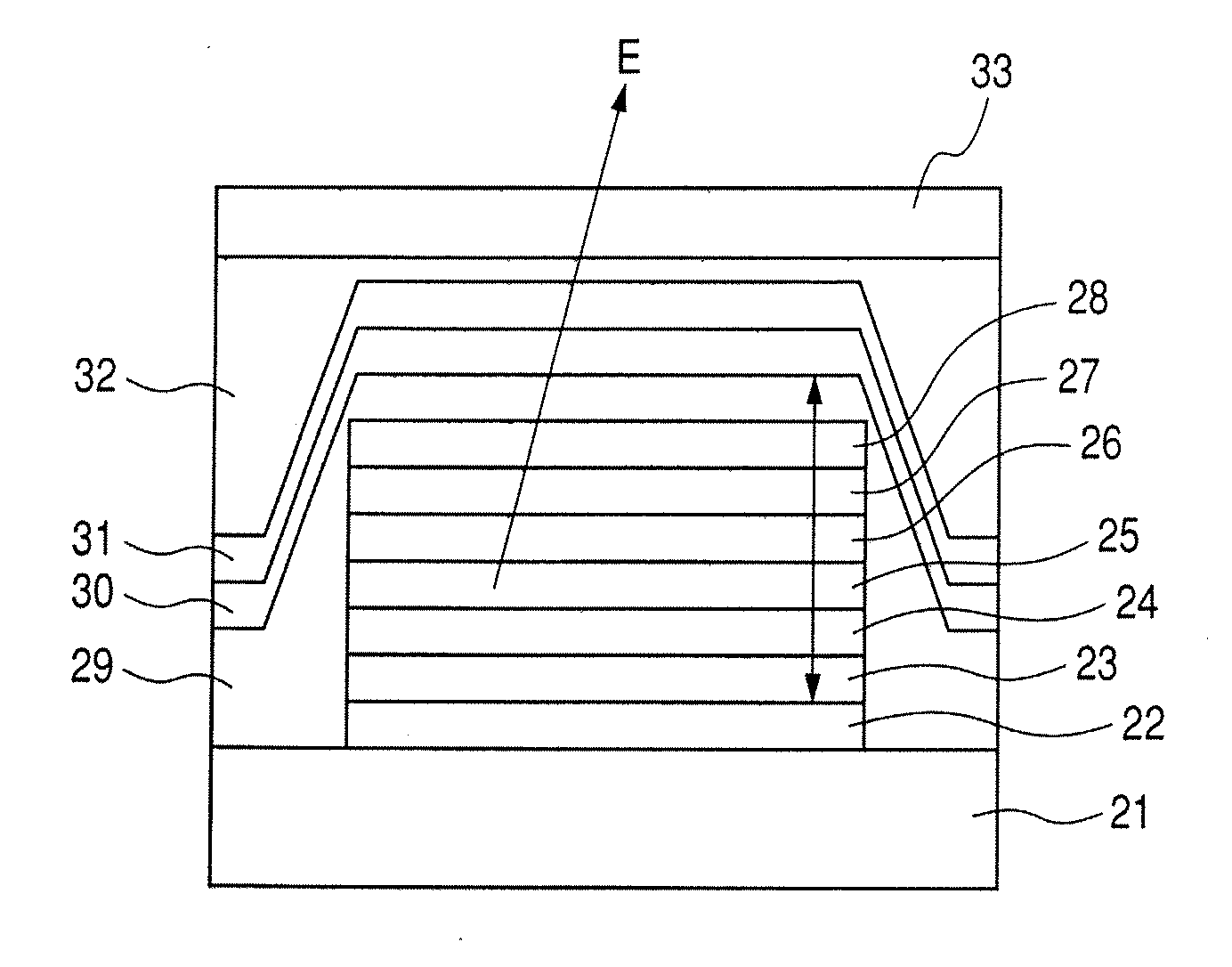
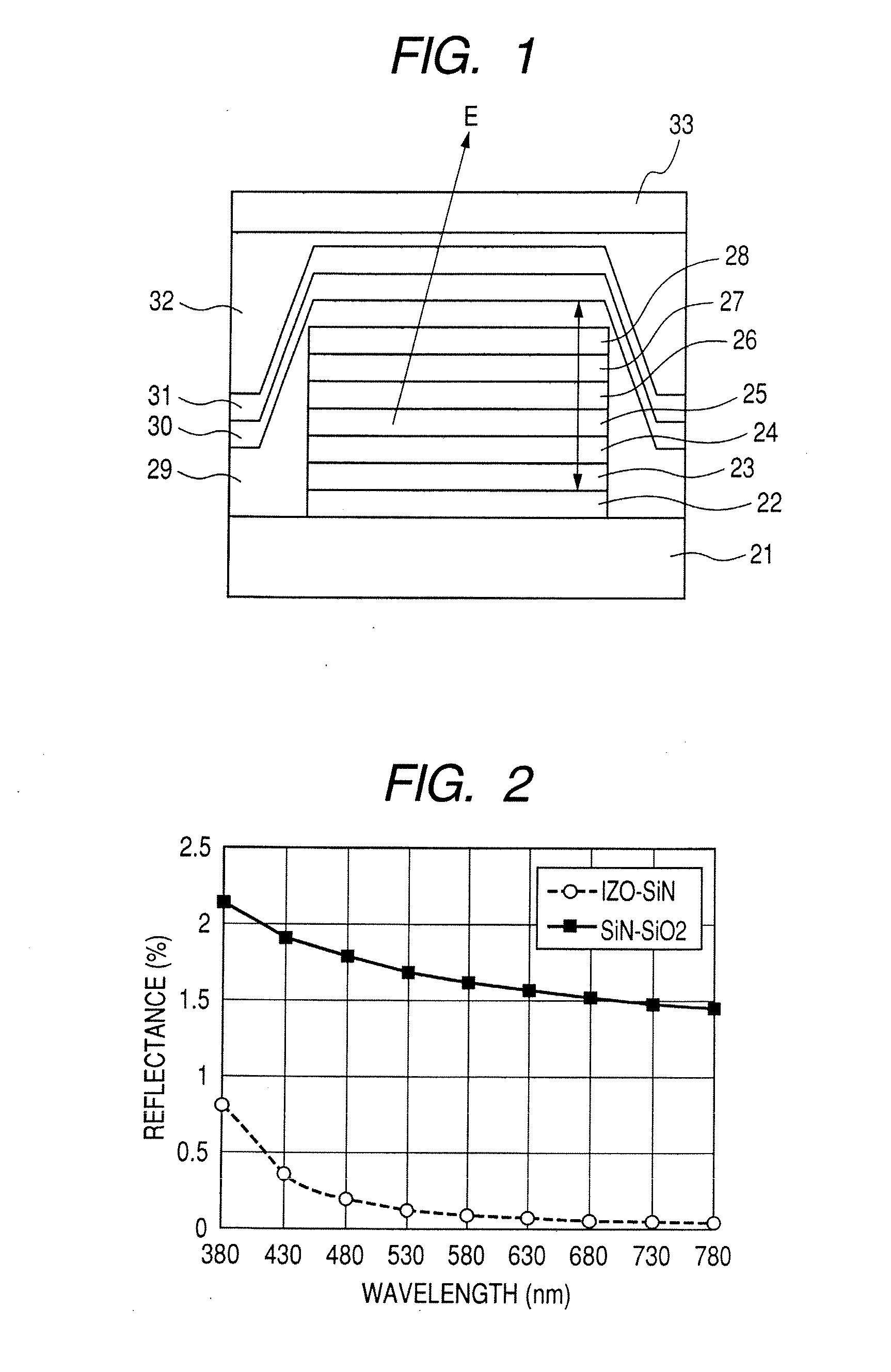
[0098]The organic light-emitting device having the structure illustrated in FIG. 1 was produced by the method described below. On a glass substrate 21, silver alloy (AgCuNd) having a film thickness of approximately 100 nm serving as the reflective electrode 22 and IZO having a film thickness of 10 nm serving as the transparent conductive layer 23 were formed by sputtering. This substrate was ultrasonically cleaned with isopropyl alcohol (IPA), washed with boiled water, and then dried. Further, after being cleaned with UV / ozone, organic compound layers were formed by a vacuum evaporation method.

[0099]First, as the hole-transporting layer 24, a film of Compound (I) represented by the following structure formula was formed in a thickness of 10 nm. At that time, the degree of vacuum was 1×10⁻⁴ Pa, while the evaporation rate was 0.2 nm / sec.

[0100]Then, as the emission layer 25 that emits blue light, a film was formed in a thickness of 20 nm by coevaporation of Compound (II) shown below as...

example 2

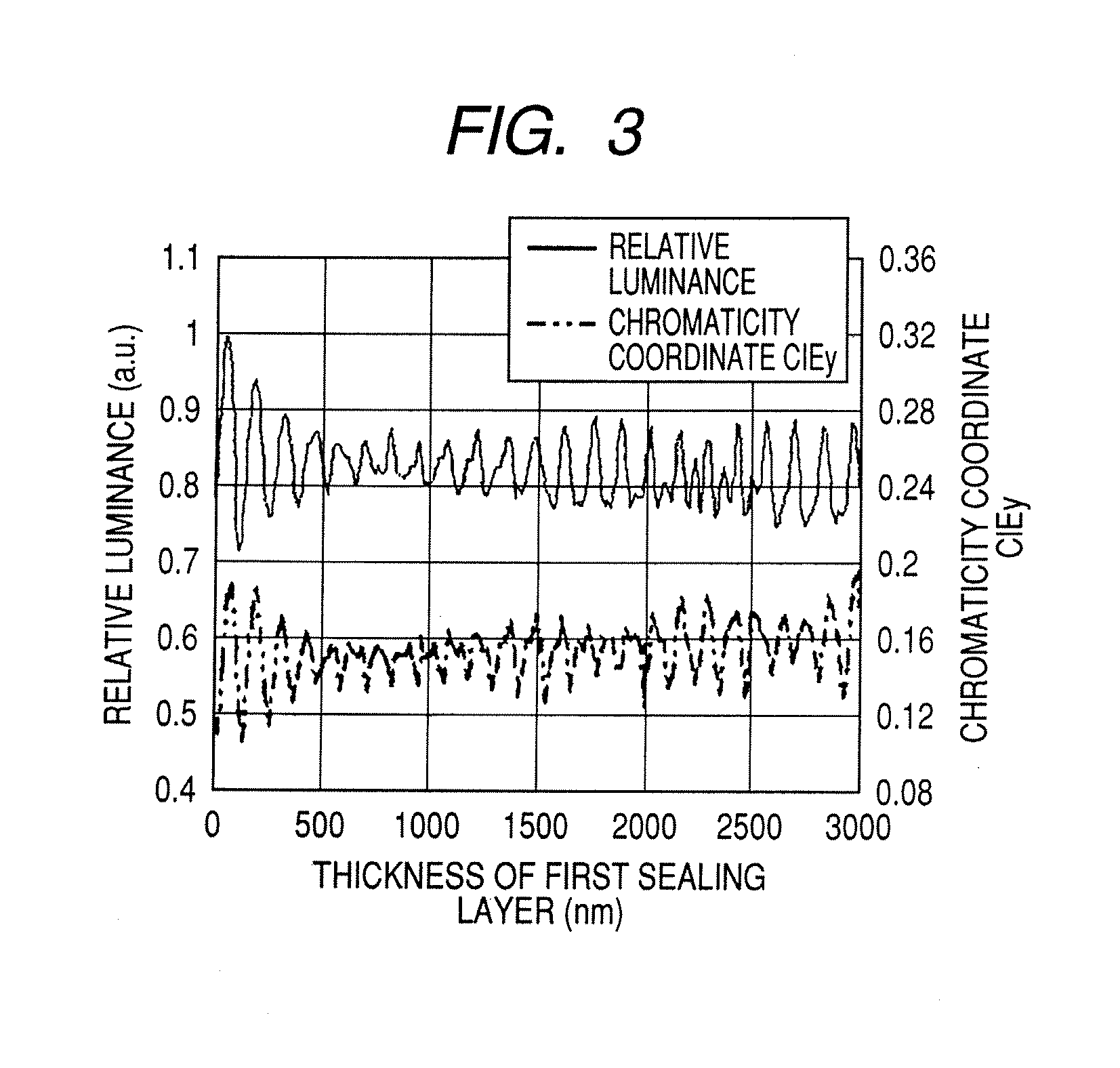
[0111]In the present example, an organic light-emitting device was produced by following the same procedure as in Example 1 with the exception that the film thickness of the first sealing layer was 1,000 nm.

[0112]As shown in Table 12, according to this organic light-emitting device, an organic light-emitting device that has stable emission characteristics and exhibits excellent light emission even when a film thickness fluctuation occurs can be produced in a simple process with a satisfactory throughput.

example 3

[0117]A display apparatus of three colors of RGB having the structure shown in FIG. 8 was produced by the method described below.

[0118]On a glass substrate 101 serving as a support member, a TFT drive circuit 102 including a low temperature polysilicon was formed, and a planarizing film 103 of an acrylic resin was formed thereon, whereby a substrate was obtained. Then, on the substrate, a film of a silver alloy (AgCuNd) as a reflective metal 104 was formed in a thickness of approximately 100 nm by a sputtering method and patterned. The reflective metal 104 was electrically connected to the TFT drive circuit 102 through contact holes 105. After that, a film of IZO as a transparent conductive layer 106 was formed in a thickness of 10 nm by a sputtering method and patterned. Further, a device separation film 107 was formed using an acrylic resin. This substrate was ultrasonically cleaned with isopropyl alcohol (IPA), washed with boiled water, and then dried. Further, after being cleane...


PUM


Abstract

Provided is a thin organic light-emitting device which exhibits satisfactory emission characteristics and is hardly affected by film thickness fluctuation in individual layers and exhibits stable emission characteristics and which includes a substrate, a first electrode provided on the substrate, an organic compound layer provided on the first electrode, a second electrode provided on the organic compound layer, and a first sealing layer provided on the light extraction side of the second electrode, in which an optical distance between a first reflective surface located on the substrate side and a second reflective surface located on the sealing layer side is adjusted so as to form a resonance portion of a resonator structure for resonating light emitted from the organic compound layer, and in which the second reflective layer is an interface on the light extraction side of the first sealing layer.

Description

BACKGROUND OF THE INVENTION[0001]1. Field of the Invention[0002]The present invention relates to a light-emitting device using an organic compound and a display apparatus using the device, and more specifically, to an organic light-emitting device (hereinafter, also simply referred to as device) that emits light when an electric field is applied to a thin film made of an organic compound, and a display apparatus using the device.[0003]2. Description of the Related Art[0004]Research and developmental works are now carried out actively on organic light-emitting devices (organic EL devices or organic electroluminescent devices). In such organic EL devices, typically, moisture or oxygen in an external environment causes deterioration of an organic compound, deterioration and peeling of an electrode / organic-substance interface, oxidization of electrodes, and the like. This results in a reduction of emission luminance, an increase of a driving voltage, generation and growth of a non-emiss...

Claims


Application Information

Patent Timeline
Patent Type & Authority Applications(United States)
IPC IPC(8): H01L27/32H01J1/62
CPCH01L51/5237H01L2251/5315H01L51/5265H10K50/841H10K50/844H10K50/852H10K2102/3026
Inventor HASEGAWA, TOSHINORIIZUMI, NOZOMU
Owner CANON KK
Why Eureka
Try Eureka