Method for Ultimate Noise Isolation in High-Speed Digital Systems on Packages and Printed Circuit Boards (PCBS)

a technology of digital systems and printed circuit boards, applied in the direction of pulse manipulation, pulse technique, electrical apparatus contruction details, etc., can solve the problems of unfavorable power distribution in computer systems, power supply noise, delta-i noise, and simultaneous switching noise, etc., to achieve excellent isolation and improve noise isolation

Inactive Publication Date: 2008-08-28
IBM CORP
View PDF8 Cites 21 Cited by
  • Summary
  • Abstract
  • Description
  • Claims
  • Application Information

AI Technical Summary

Benefits of technology

[0011]Improved noise isolation for high-speed digital systems on packages and printed circuit boards (PCBs) is provided by the use of power island and mixed (or hybrid) alternating impedance electromagnetic bandgap (AI-EBG) structures configured to provide ultimate noise isolation (i.e., from DC to a substantially infinite frequency). A power island is surrounded by a plurality of mixed AI-EBG structures to provide a power distribution network. In this structure, the gap around the power island provides excellent isolation from DC to the first cavity resonant frequency. One AI-EBG structure (type I) provides excellent isolation from the first cavity resonant frequency of around 1.5 GHz to about 5 GHz. The other AI-EBG structure (type II) provides excellent isolation from about 5 GHz to 10 GHz. Through use of this novel configuration with mixed AI-EBG structures and a power island, a combination effect of the hybrid AI-EBG structure (i.e., the unique combination of type I and type II structures) provides excellent isolation far in excess of 10 GHz. The AI-EBG structure is a metallic-dielectric EBG structure that comprises two metal layers separated by a thin dielectric material (similar to power / ground planes in packages and PCBs). However, in the AI-EBG structure, only one of these metal layers has a periodic pattern which is a two-dimensional (2-D) rectangular lattice with each element consisting of a metal patch with four connecting metal branches.

Problems solved by technology

A combination of voltage scaling and Moore's law is causing an alarming increase in the power consumed by microprocessors.
This trend in microprocessors is causing a major challenge for distributing power in computer systems.
A major contribution to power supply noise comes from the package and board level interconnections.
This undesired voltage fluctuation on the power / ground planes is commonly known as simultaneous switching noise (SSN), power supply noise, and delta-I noise.
Power supply noise leads to unwanted effects on PDN such as ground bounce, false triggering in digital circuits, and waveform distortion in the time domain.
Especially, power supply noise can be transferred to anywhere in power / ground planes in packages and boards since power / ground planes behave as a parallel-plate waveguide at high frequencies.
However, real power and ground planes have the finite size of the width and length, which means that waves propagating to the edges of the power / ground planes have to be reflected back and forth.
Hence, this method only provides a marginal isolation (−20 dB˜−60 dB) at high frequencies (usually above ˜1 GHz) and could create a serious problem as the sensitivity of digital circuits increases and the operating frequency of the system increases.
Generally, split planes provide good isolation (−70 dB˜−80 dB) at low frequencies (usually below ˜1 GHz) but show poor isolation (−20 dB˜−60 dB) at high frequencies because of electromagnetic coupling.
In these EBG structures, the constructive and destructive interference of electromagnetic waves results in transmission and reflection bands.
However, this type of AI-EBG structure only provides excellent isolation in high frequency range but does not provide excellent isolation in DC and low and mid frequency ranges.

Method used


Image

  • Method for Ultimate Noise Isolation in High-Speed Digital Systems on Packages and Printed Circuit Boards (PCBS)
  • Method for Ultimate Noise Isolation in High-Speed Digital Systems on Packages and Printed Circuit Boards (PCBS)
  • Method for Ultimate Noise Isolation in High-Speed Digital Systems on Packages and Printed Circuit Boards (PCBS)

Examples


Embodiment Construction

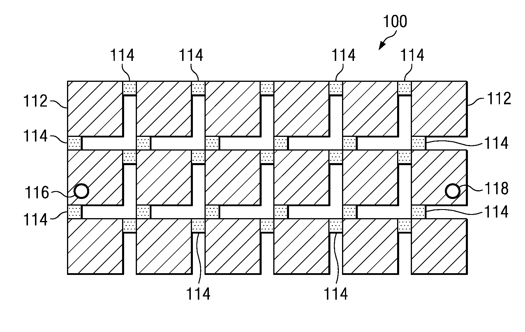
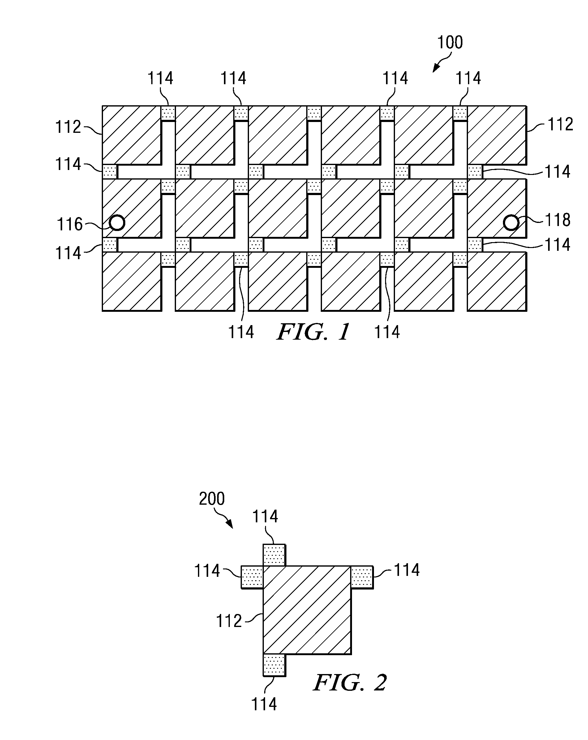
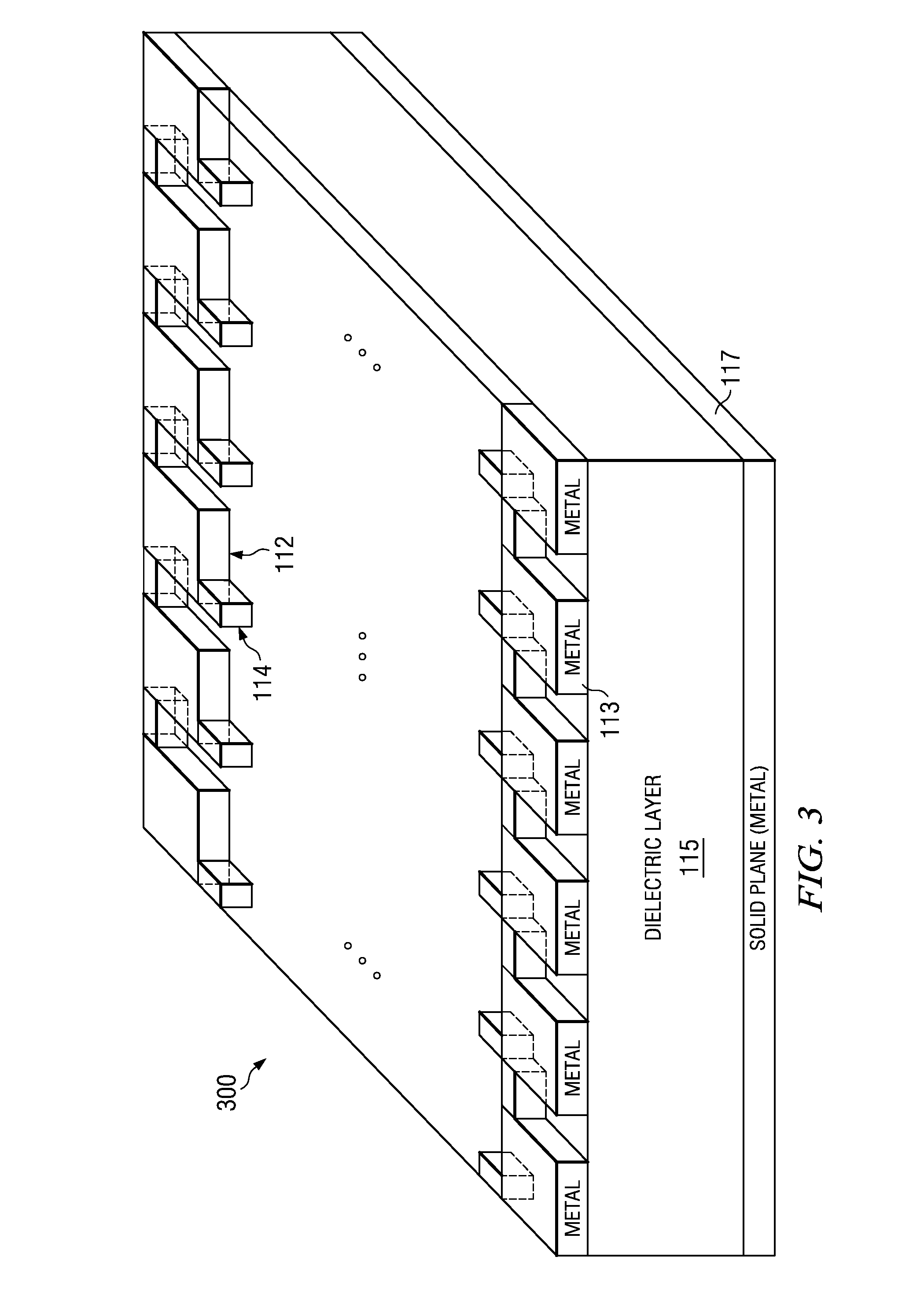
[0028]Referring now to the figures and in particular to FIG. 1, there is shown one type of AI-EBG structure that provides noise isolation for a wide frequency range in high frequency. FIG. 1 illustrates a top view of one embodiment of a system having an AI-EBG structure 100. The AI-EBG structure 100 has an AI-EBG plane that includes a plurality of first elements 112 continuously connected by a plurality of second elements 114 in the same dimensional plane (not all of the first and second elements are labeled in FIG. 1, in order to not obscure details of the figure). The first elements 112 have relatively low characteristic impedance and the second elements 114 have relatively high characteristic impedance to thus provide a multiple alternating impedance electromagnetic bandgap (AI-EBG) structure. At first location 116 and second location 118, the AI-EBG plane can also be coupled to supply power / ground to various devices or circuits. At first location 116, the AI-EBG plane can be cou...


PUM


Abstract

Improved noise isolation for high-speed digital systems on packages and printed circuit boards is provided by the use of mixed alternating impedance electromagnetic bandgap (AI-EBG) structures and a power island configured to provide ultimate noise isolation. A power island is surrounded by a plurality of mixed AI-EBG structures to provide a power distribution network. In this structure, the gap around the power island provides excellent isolation from DC to the first cavity resonant frequency which is determined by the size of the structure and dielectric material. One AI-EBG structure provides excellent isolation from the first cavity resonant frequency of around 1.5 GHz to 5 GHz. The other AI-EBG structure provides excellent noise isolation from 5 GHz to 10 GHz. Through use of this novel configuration of AI-EBG structures, a combination effect of the hybrid AI-EBG structure provides excellent isolation far in excess of 10 GHz. The AI-EBG structure is a metallic-dielectric EBG structure that comprises two metal layers separated by a thin dielectric material (similar to power / ground planes in packages and PCBs). However, in the AI-EBG structure, only one of the metal layers has a periodic pattern which is preferably a two-dimensional rectangular lattice with each element consisting of a metal patch with four connecting metal branches.

Description

RELATED APPLICATION[0001]This application is related to co-pending U.S. patent application entitled “Mixed-signal systems with alternating impedance electromagnetic bandgap (ai-ebg) structures for noise suppression / isolation” having Ser. No. 11 / 260,952, filed on Oct. 28, 2005, and which is entirely incorporated herein by reference as background material.BACKGROUND[0002]1. Field of the Invention[0003]The present disclosure is generally related to a noise isolation technique useful in high-speed digital systems on packages and printed circuit boards (PCBs), collectively referred to herein as a component carrier, and more particularly is related to electromagnetic bandgap structures that provide ultimate noise isolation (i.e., from DC to a substantially infinite frequency).[0004]2. Description of the Related Art[0005]Over the last decade, the scaling of the CMOS transistors has enabled the design of microprocessors operating at multi-gigahertz frequencies. This trend, based on the Inte...

Claims


Application Information

Patent Timeline
Patent Type & Authority Applications(United States)
IPC IPC(8): H03B1/04
CPCH05K1/0236H05K1/167H01Q15/006H05K2201/09309H05K2201/09681H05K3/4641H05K1/02
Inventor CHOI, JINWOO
Owner IBM CORP
Why Eureka
Try Eureka