Plasma process for inductively coupling power through a gas distribution plate while adjusting plasma distribution

a plasma process and plasma technology, applied in plasma techniques, fluid pressure measurement, instruments, etc., can solve the problems of uniform gas distribution, non-uniform plasma density, and inability to meet the requirements of production, so as to increase the reaction rate and etch rate, increase the dissociation in the plasma, and increase the ion density

Inactive Publication Date: 2008-08-28
APPLIED MATERIALS INC
View PDF10 Cites 25 Cited by
  • Summary
  • Abstract
  • Description
  • Claims
  • Application Information

AI Technical Summary

Benefits of technology

[0002]One limitation of such reactors is that not all process parameters can be independently controlled. For example, in an inductively coupled reactor, in order to increase reaction (etch) rate, the plasma source power must be increased to increase ion density. But, this increases the dissociation in the plasma, which can reduce etch selectivity and increase etch microloading problems, in some cases. Thus, the etch rate must be limited to those cases where etch selectivity or microloading is critical.
[0003]Another problem arises in the processing (e.g., etching) of multi-layer structures having different layers of different materials. Each of these layers is best processed (e.g., etched) under different plasma conditions. For example, some of the sub-layers may be best etched in an inductively coupled plasma with high ion density and high dissociation (for low mass highly reactive species in the plasma). Other layers may be best etched in a capacitively coupled plasma (low dissociation, high mass ions and radicals), while yet others may be best etched in plasma conditions which may be between the two extremes of purely inductively or capacitively coupled sources. However, to idealize the processing conditions for each sub-layer of the structure being etched would require different process reactors for each of the different sub-layers, and this is not practical.
[0004]Gas distribution is most effectively controlled by injecting the process gas into the reactor chamber through a gas distribution showerhead forming a portion of the ceiling overlying the wafer pedestal. Inductively coupled power distribution across the wafer is most effectively controlled by providing a

Problems solved by technology

In semiconductor fabrication processes, conventional sources of plasma source power, such as inductively coupled RF power applicators or capacitively coupled RF power applicators, introduce inherent plasma density non-uniformities into the processing.
As device geometries have continued to shrink, such non-uniformities become more critical, requiring better compensation.
However, a large ceiling-to-wafer distance can prevent the beneficial gas distribution effects of a ceiling gas distribution showerhead from reaching the wafer surface, due to diffusion over the large distance.
In summary, the wafer-ceiling gap is optimized for ion density uniformity, which may not necessarily lead to uniform gas distribution.
One limitation of such reactors is that not all process parameters can be independently controlled.
But, this increases the dissociation in the p

Method used


Image

  • Plasma process for inductively coupling power through a gas distribution plate while adjusting plasma distribution
  • Plasma process for inductively coupling power through a gas distribution plate while adjusting plasma distribution
  • Plasma process for inductively coupling power through a gas distribution plate while adjusting plasma distribution

Examples


third embodiment

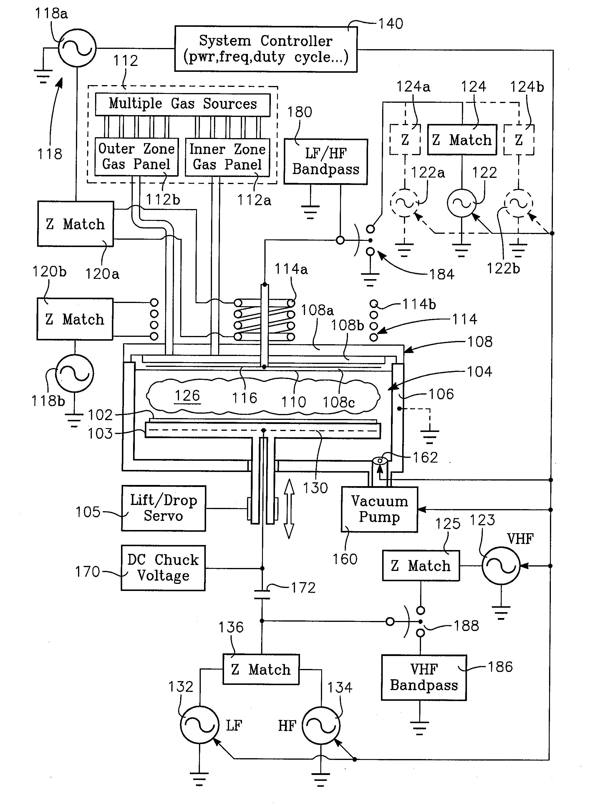
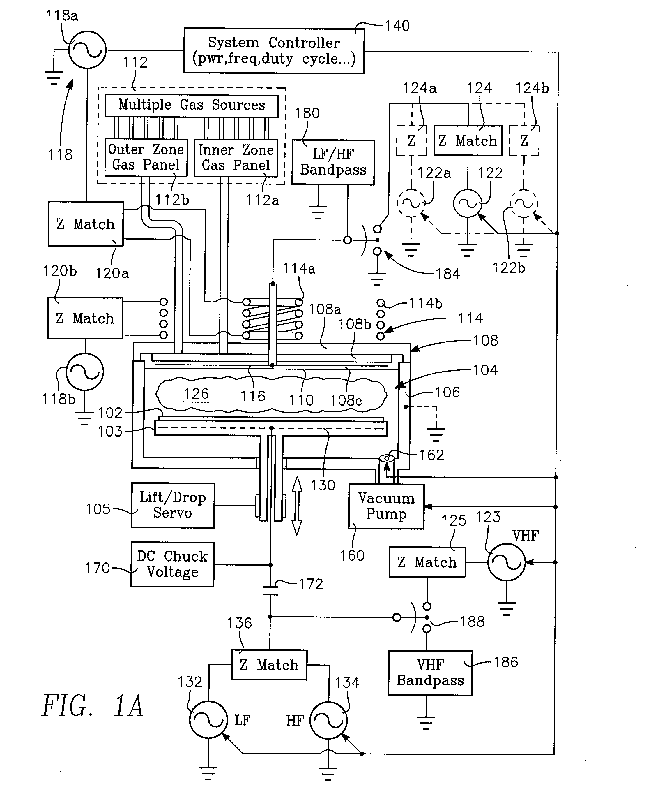
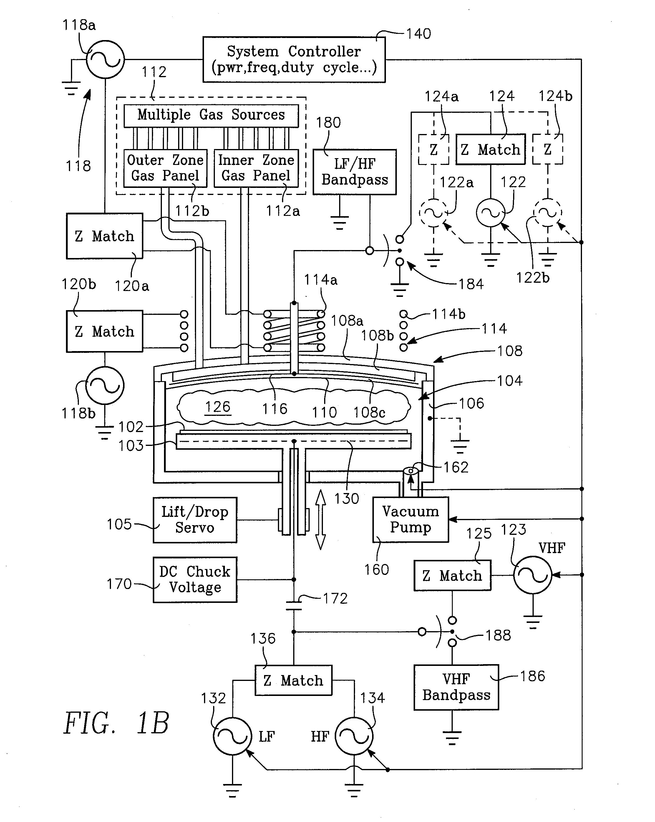
[0053]The RF power generator 118 (or the generators 118a, 118b) provides high frequency (HF) power (e.g., within a range of about 10 MHz through 27 MHz). In one embodiment in which the ceiling electrode 116 is the capacitively coupled source power applicator, an RF power generator 122 provides very high frequency (VHF) power (e.g., within a range of about 27 MHz through 200 MHz) through an impedance match element 124 to the capacitively coupled power applicator 116. In another embodiment in which the bottom (workpiece support) electrode 130 is the capacitively coupled source power applicator, an RF power generator 123 provides VHF power through an impedance match element 125 to the bottom electrode 130. In a third embodiment, both the ceiling and bottom electrodes 116, 130 comprise the capacitively coupled plasma source power applicator, so that both VHF generators 122, 123 are present. In a further embodiment, both electrodes 116, 130 are present, but VHF plasma source power is app...

first embodiment

[0056]In the first embodiment, VHF power is applied only to the ceiling electrode 116. In this case, it may desirable for the workpiece support electrode 130 to function as the return path for the VHF power applied to the ceiling electrode 116 and for the ceiling electrode to function as the return path for the HF power applied to the workpiece support electrode 130. For this purpose, the ceiling electrode 116 may be connected through an LF / HF bandpass filter 180 to ground. The bandpass filter 180 prevents VHF from the generator 122 from being diverted from the ceiling electrode 116 to ground. Similarly, the wafer support electrode 130 may be connected (via the RF isolation capacitor 172) to ground through a VHF bandpass filter 186. The VHF bandpass filter 186 prevents LF and HF power from the generators 132, 134 from being diverted from the electrode 130 to ground.

[0057]In the second embodiment, VHF power is applied to only the wafer support electrode 130. In this case, the wafer s...


PUM

PropertyMeasurementUnit
Lengthaaaaaaaaaa
Timeaaaaaaaaaa
Poweraaaaaaaaaa

Abstract

A method of processing a workpiece in the chamber of a plasma reactor having a ceiling overlying the workpiece by introducing a process gas into the chamber through a gas distribution plate in the ceiling. The gas is introduced by distributing gas flow from a first gas input to plural gas distribution orifices extending through a manifold of the gas distribution plate, and distributing gas flow from each of the plural gas distribution orifices to plural gas injection orifices in a showerhead of the gas distribution plate. The method further includes restricting gas flow in the gas distribution plate to paths having arcuate lengths about an axis of symmetry less than a complete circle. The method also includes capacitively and inductively coupling plasma source power into the chamber through the gas distribution. The method further includes adjusting the plasma ion density radial distribution in the process region by adjusting the ratio between the amounts of the capacitively coupled VHF power and the inductively coupled power.

Description

BACKGROUND OF THE INVENTION[0001]In semiconductor fabrication processes, conventional sources of plasma source power, such as inductively coupled RF power applicators or capacitively coupled RF power applicators, introduce inherent plasma density non-uniformities into the processing. In particular, inductively coupled plasma sources are characterized by an “M”-shaped radial distribution of plasma ion density over the semiconductor workpiece or wafer. As device geometries have continued to shrink, such non-uniformities become more critical, requiring better compensation. Presently, the non-uniformity of an overhead inductively coupled source is reduced or eliminated at the wafer surface by optimizing the coil design and the ceiling-to-wafer distance of the chamber. This distance must be sufficient so that diffusion effects can overcome the effects of the non-uniform ion distribution in the ion generation region before they reach the wafer. Generally, for an inductively coupled plasma...

Claims


Application Information

Patent Timeline
IPC IPC(8): H05H1/00
CPCC23C16/505H01J37/32082H01J37/3244H01J37/321H01J37/32091
Inventor PATERSON, ALEXANDERTODOROV, VALENTIN N.PANAGOPOULOS, THEODOROSHATCHER, BRIAN K.KATZ, DANHAMMOND, EDWARD P.HOLLAND, JOHN P.
Owner APPLIED MATERIALS INC
Why Eureka
Try Eureka